
The completion of Berlin Brandenburg International Airport (BER) once again being postponed is no longer newsworthy. As recently as late last year, further delays were anticipated according to the Berliner Morgenpost. This time it wasn't about the completion of the airport itself though, but about the opening of the various duty-free shops, cafés and other establishments that were scheduled to start operating as soon as the airport was ready. However, the airport company told the Berliner Morgenpost that conductor rails needed replacing, causing further delay. What happened? Apparently, a manufacturing defect with the conductor rails caused a problem that suppliers of electronic materials and manufacturers of electronic components are faced with from time to time: whisker formation. Whisker formation on tin-surfaces is a phenomenon known since the 1950s. It was never researched thoroughly, as the solution back then was to add lead to the tin-surface. But ever since the European Union adopted legislative measures in July 2006 to prohibit lead in electronic components, whisker formation once again became an issue.
Whiskers are crystalline, hair-thin excretions that can grow several millimeters long. They may reduce the insulation resistance and/or the distance between adjacent components. If they break, they may cause short circuits on the circuit board or for fine-pitch components. However, the biggest challenges are caused by electric arcs, which can occur at high currents and voltages. The specific conditions required for whisker formation have not yet been fully explored. But it appears that the risk is particularly high if a copper surface is covered with pure tin.
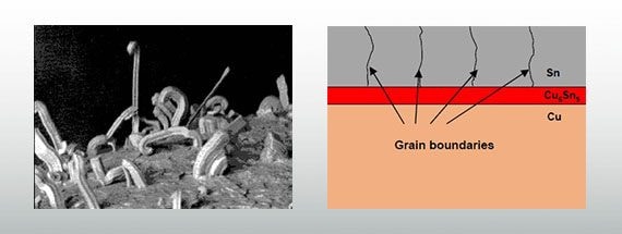
Illustration 1: Compressive stress due to grain boundary diffusion
The most common theories are that whiskers form under varying ambient conditions (temperature, humidity, air pressure), that they grow from the base – and thus directly from the substrate – and that they are caused by compressive stress in the tin layers: at room temperature, an intermetallic layer (Cu6Sn5) forms at the boundary surface between copper and tin. At temperatures below 60°C, the mass diffusion from the CuSn phase is significantly lower than the grain-boundary diffusion. That is why the intermetallic phase increasingly fills the grain boundaries which causes the rise of the compressive stress in the Sn-grains.
Due to an increased lattice spacing, the Cu6Sn5 phase requires more space than the original material. These changes in the lattice cause compressive stress on the tin layer. This compressive stress is relieved by mass transport from the tin layer and leads to the formation of whiskers, which mainly originates from small defects (illustration 1). Tin oxide causes a similar effect on the top side of the tin. Because SnO2 and SnO require more space than tin on its own, humidity and corrosion, which penetrate the grain boundaries from above, also cause compressive stress. Contamination increases this effect because of its tendency to oxidation – thus electroplated layers are also very susceptible to whisker formation. Consequently, the chemicals used and the tinning process itself have a direct impact on the tendency to form whiskers. External compressive stress, as caused by bending, scratches or twisting, have an impact on the formation of whiskers as well.
Based on these theories, it is apparent that stress in tin-plated materials needs to be avoided to reduce whisker formation. Therefore, it may help to:
Würth Elektronik consistently takes these factors and other recommendations into account to minimize the risk of whisker formation. Additionally, we perform three proven whisker tests to verify the quality of selected coatings.
You can find more detailed information about whisker formation and how we deal with it in our application note.

