Efficient use of space and high power
The future of electronics is tending towards higher reliability, more functions and increasing miniaturization. Efficient use of shrinking package volumes and tiny surfaces is becoming increasingly important. The spectrum of applications ranges from the automotive industry and industrial electronics to medical technology and sensor technology.
Embedding technology serves as a solution for reduced installation space. Active or passive components are brought into the printed circuit board using an embedding process so that they are completely integrated into the structure. We distinguish between four manufacturing processes:
Advantages of Würth Elektronik embedding technology
Relevant parameters for production-ready PCB design
Modern printed circuit board solutions are more than just connecting elements. They are the key to progress in electronics. With this in mind, we actively support our customers in development and also offer our own system solutions with electronic.
The Embedding design rules include all the important parameters you need to make your project successful:
In our Embedding design guide you will find an overview of all variants. In addition, our specialists have summarized valuable design tips for you here. This will help you bring your application to success reliably and safely.
Would you like to download our design guides and design rules as a clear technology poster? The poster provides you with the most important information about efficient PCB design.
Dive playfully into the world of our Embedding technology and gain a deeper understanding
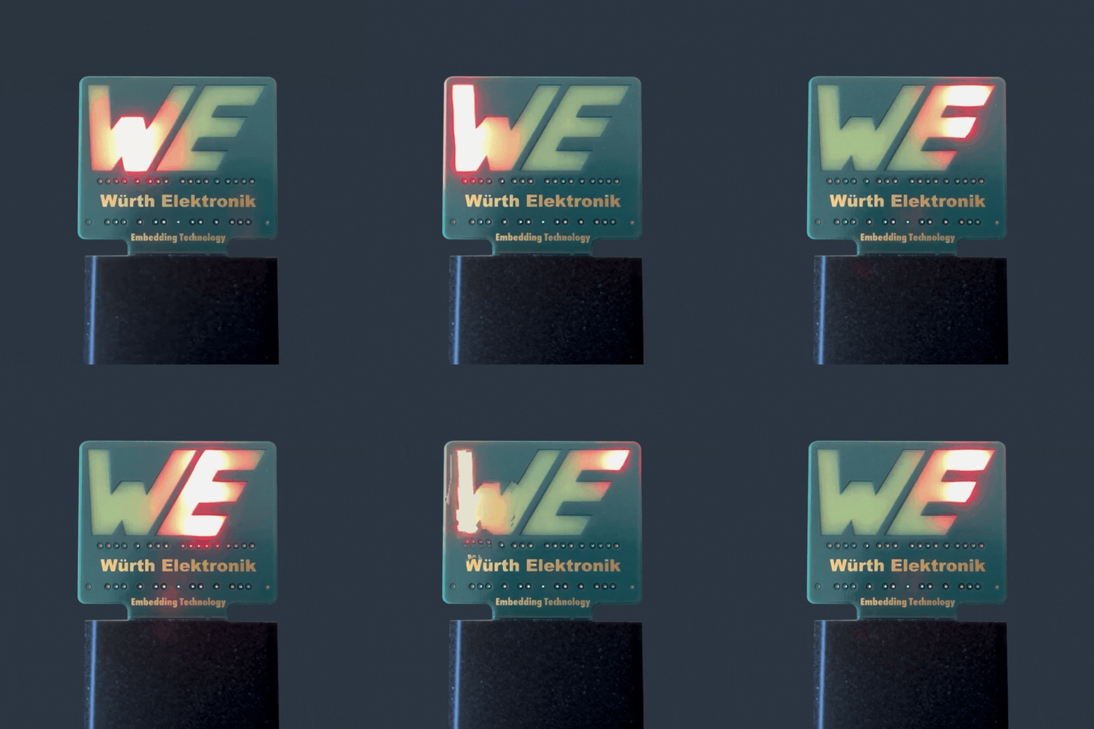
Our DEVICE.embedding prototype WE.embed showcases a functioning assembly with active and passive components embedded in the SOLDER.embedding variant. Simply plug the prototype into a USB 2.0 port and let the WE logo shine!
Embedding technology
Take a look at the recordings or the presentations of the webinars:
'The world of embedded components in printed circuit boards - Basics - part 1'
'The world of embedded devices in printed circuit boards - Layout and applications - part 2'
'Miniaturization, function, reliability: DEVICE.embedding physical PCB sample WE.embed'
Webinar "The world of embedded components in printed circuit boards - Basics - part 1"
Contact us


