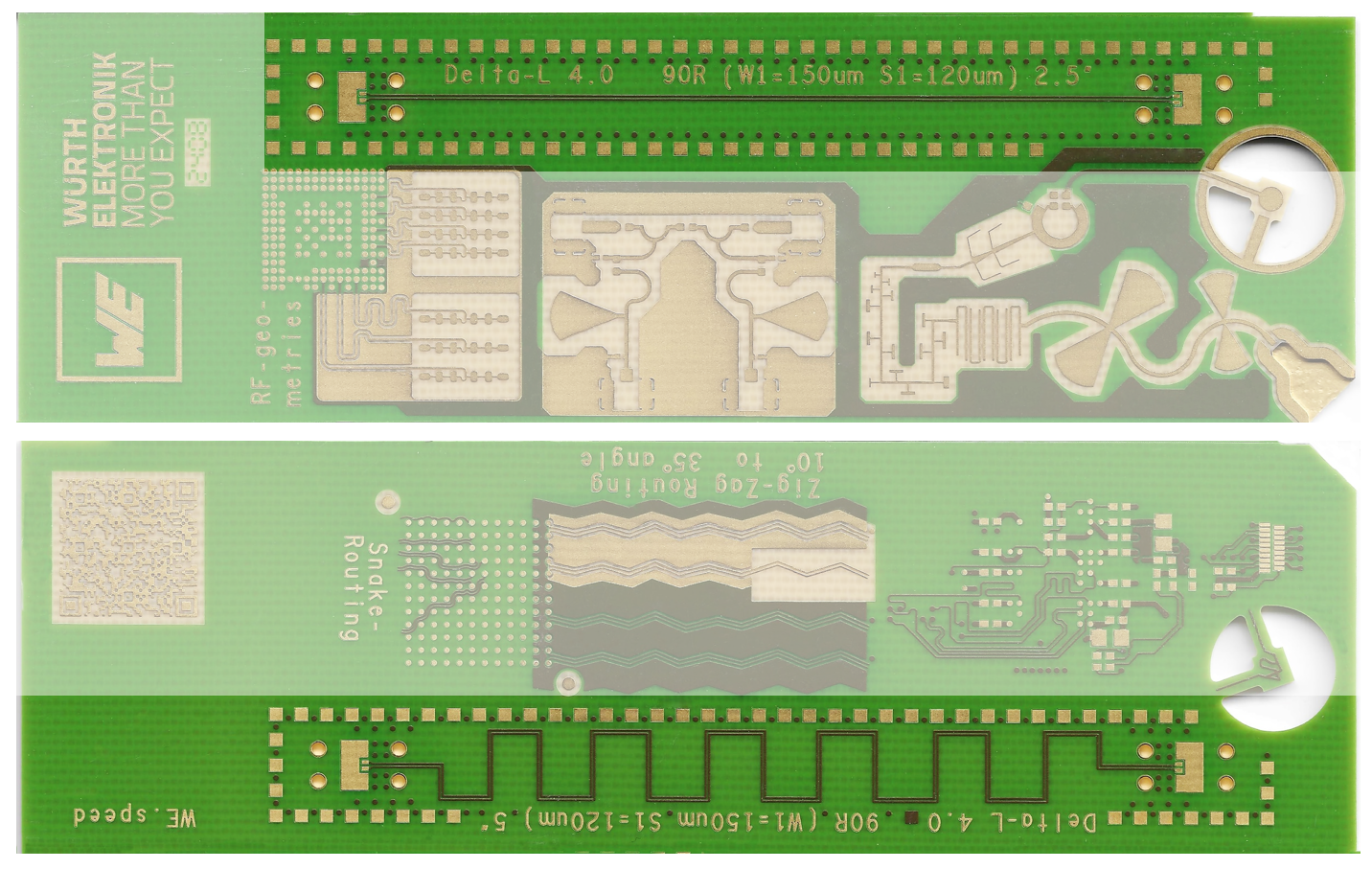
HIGH.speed Sample WE.speed
The world around us is getting faster and faster and electronic devices with WiFi 6, DDR5, PCIe or USB4 are coming onto the market. In many industrial applications, the tried and tested FR4 material can still provide the necessary performance.
However, modern interfaces such as memory connections or high-resolution video signals are pushing the standard PCB material to its limits. It is therefore necessary to make adjustments to the design and manufacture of the PCB in order to achieve maximum performance with good signal integrity in the product.
This hand sample demonstrates some of these adaptations.
Description: The material parameters in the data sheet have been carefully determined, but the final parameters differ due to the real influence of layout, tolerances and environmental conditions. In order to determine these parameters precisely, test coupons are used, which are helpful during development but also for series monitoring.
Explanations: The implemented coupon shows a Delta-L 4.0 measurement coupon. It is a further development of the classic impedance coupons, with which the dielectric constant (Dk) and the Dissipation Factor (Df) can also be determined. This requires two measuring sections of different lengths, which are implemented here on the front and back with little space required.
Explanations: In this area some typical antenna structures are shown. In order to ensure good transmission Tx and reception Rx quality, the antenna structures must be precisely adapted. Simulations are essential here for an optimal signal-to-noise ratio. If you need support with this, the WEdesign team can provide support as a service.
Design: A typical circuit for a mmWave sensor device is shown in this area.
Explanation: The 3 Tx and 4 Rx structures on the circuit board send and receive the signal in the 60 Ghz range, while the signal is processed in the BGA processor and can then be passed on digitally.
Design: Complex HDI structures are also possible with HIGH.speed materials. Apply the proven BASIC and HDI design rules.
Explanation: Complex setups such as a 2+10b+2 are also possible. Please contact us early about an impedance-adapted layer structure.
Design: Zig-Zag routing to optimize signal transit time.
Explanation: To ensure that two signals reach the receiver at the same time, Zig-Zag routing helps adjust the signal transit time. The transit time of the signals depends on material parameters such as the dielectric constant Dk. Since the materials used like glass fibers and resin, have different values, Zig-Zag routing avoids unwanted effects. Please see the webinar for further details.


