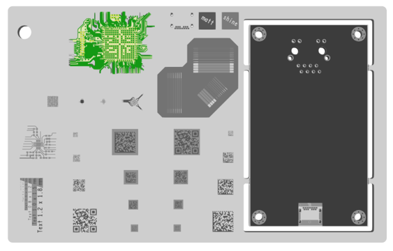
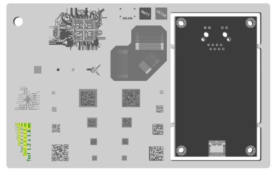
Physical PCB sample "Digital solder mask"
Sample for the presentation “Design rules for digital solder mask - what are the current possibilities?” at the FED conference on 18.09.2024
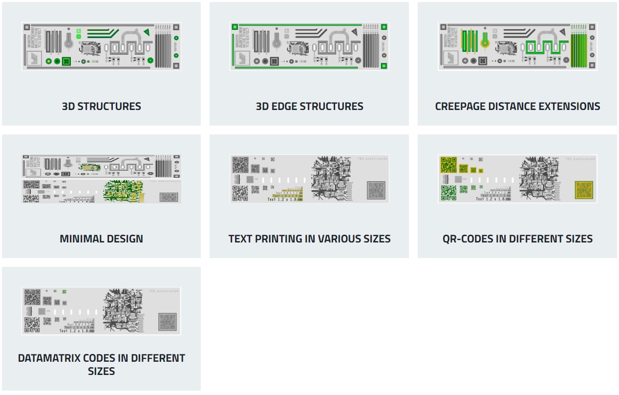
This hand sample demonstrates the new possibilities of additively applied solder mask, also known as s.mask. An outstanding new feature is 3D printing in height. In a similar way to conventional 3D printing with materials such as PLA or ABS, the solder mask is applied in layers with a thickness of around 40 μm per layer. However, extremely steep edges cannot be realized. A certain gradation of the flanks is necessary. In this way, structure heights of up to 1400 μm (1.4 mm) can be achieved.
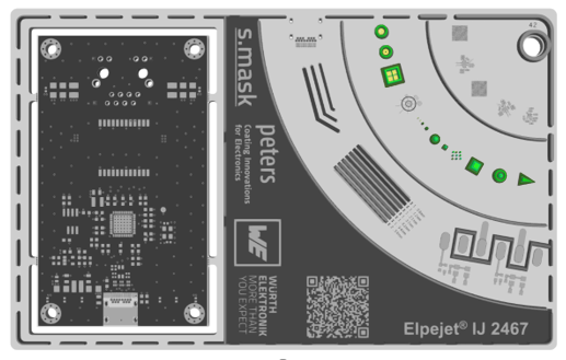
Design/description: 3D structures highlighted here can serve a variety of purposes. They can be used as graphic elements, such as a brand or company logo or branding. If only frames are printed, these can be used as protective elements or casting frames. Individual bodies can be used, for example, as mechanical structures or as supports and spacers for a wide range of requirements.
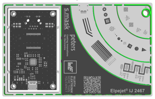
Description: Elements highlighted here serve, for example, to protect more delicate elements on the surfaces between them. With minimal structure widths, these fine elements must be protected against damage from heavy mechanical stress, such as during handling (transport at the PCB manufacturer or EMS).
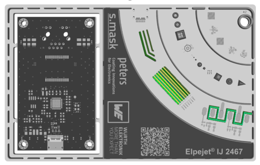
Description: These elements are used to increase the creepage distance between adjacent conductive areas and elements on the surface of the printed circuit board. This means, for example, that the creepage distance can be significantly increased while maintaining the same distance between conductive areas on the surface of the printed circuit board. This requires an increase and thus a lengthening of the distance in the Z-axis using acrylic lacquer.
Furthermore, the additive solder resist application process also makes it possible to selectively increase the coverage at the conductor track edges in certain areas.
Description: With additive printing technology, it is sufficient to print lacquer only on the areas of the design that need to be protected and covered (copper traces and areas). This significantly reduces the amount of solder resist required and greatly improves the CO2 footprint.
Description: The very small drop size allows minimal structures to be printed. The limits were deliberately not quite reached on the hand sample. However, character sizes of 0.4 x 0.63 mm are entirely conceivable.
Contact us

