Analog Devices ADP5071
2 A/1.2 A DC-to-DC Switching Regulator with Independent Positive and Negative Outputs
Details
| Topologie | Aufwärtswandler |
| Eingangsspannung | 5 V |
| Schaltfrequenz | 1130-2560 kHz |
| Ausgang 1 | 9 V / 2 A |
| IC-Revision | B |
Beschreibung
The ADP5071 is a dual high performance dc-to-dc regulator that generates independently regulated positive and negative rails.
The input voltage range of 2.85 V to 15 V supports a wide variety of applications. The integrated main switch in both regulators enables generation of an adjustable positive output voltage up to +39 V and a negative output voltage down to −39 V below input voltage.
The ADP5071 operates at a pin selected 1.2 MHz/2.4 MHz switching frequency. The ADP5071 can synchronize with an external oscillator from 1.0 MHz to 2.6 MHz to ease noise filtering in sensitive applications. Both regulators implement programmable slew rate control circuitry for the MOSFET driver stage to reduce electromagnetic interference (EMI).
Flexible start-up sequencing is provided with the options of manual enable, simultaneous mode, positive supply first, and negative supply first.
The ADP5071 includes a fixed internal or resistor programmable soft start timer to prevent inrush current at power-up. During shutdown, both regulators completely disconnect the loads from the input supply to provide a true shutdown.
Other key safety features in the ADP5071 include overcurrent protection (OCP), overvoltage protection (OVP), thermal shutdown (TSD), and input undervoltage lockout (UVLO).
The ADP5071 is available in a 20-lead LFCSP and is rated for a −40°C to +125°C junction temperature range.
Eigenschaften
- Wide input supply voltage range: 2.85 V to 15 V
- Generates well regulated, independently resistor programmable VPOS and VNEG outputs
- Boost regulator to generate VPOS output
- Adjustable positive output to 39 V
- Integrated 2.0 A main switch
- Optional single-ended primary-inductor converter (SEPIC) configuration for automatic step-up/step-down
- Inverting regulator to generate VNEG output
- Adjustable negative output to VIN − 39 V
- Integrated 1.2 A main switch
- True shutdown for both positive and negative outputs
- 1.2 MHz/2.4 MHz switching frequency with optional external frequency synchronization from 1.0 MHz to 2.6 MHz
- Resistor programmable soft start timer
- Slew rate control for lower system noise
- Individual precision enable and flexible start-up sequence control for symmetric start, VPOS first, or VNEG first
- Out-of-phase operation
- UVLO, OCP, OVP, and TSD protection
- 4 mm × 4 mm, 20-lead LFCSP and 20-lead TSSOP
- −40°C to +125°C junction temperature range
- Supported by the ADIsimPower tool set
Remarks:
- Refer page num 23 for more inductor s values.
Typische Anwendungen
- RF power amplifier (PA) bias
- Optical module supply
- Charge-coupled device (CCD) bias supply
- Bipolar amplifiers, ADCs, DACs and multiplexers
Weiterführende Informationen
Artikeldaten
| Artikel Nr. | Datenblatt | Simulation | Downloads | Status | Produktserie | L (µH) | IRP,40K (A) | ISAT,30% (A) | RDC typ. (mΩ) | fres (MHz) | VOP (V) | Montageart | Muster | |
|---|---|---|---|---|---|---|---|---|---|---|---|---|---|---|
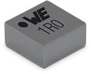 | 74438356015 | SPEC | 10 Dateien | Aktiv i| Produktion ist aktiv. Erwartete Lebenszeit: >10 Jahre. | WE-MAPI SMT-Speicherdrossel | 1.5 | 8.6 | 10.2 | 16 | 48 | 80 | SMT |
| Artikel Nr. | Datenblatt | Simulation | |
|---|---|---|---|
 | 74438356015 | SPEC |
| Muster |
|---|
| Artikel Nr. | Datenblatt | Simulation | Downloads | Status | Produktserie | L (µH) | IRP,40K (A) | ISAT,30% (A) | RDC typ. (mΩ) | fres (MHz) | VOP (V) | Montageart | Muster |
|---|


