IC-Hersteller EPC
IC-Hersteller (103)
- Alle Hersteller
 Analog Devices
 Infineon Technologies
 Microchip
 Onsemi
 Renesas
 ROHM
ROHM STMicroelectronics
 Texas Instruments
- 3peak incorporated (28)
- Ablic (23)
- Acco Semiconductor (1)
- Advanced Power (4)
- Allegro Microsystems (100)
- Alpha & Omega Semiconductor (37)
- AnalogySemi (3)
- AnDAPT Inc (204)
- Anpec (13)
- AXElite (2)
- Backward (6)
- Bright Power Semiconductor (1)
- Broadcom (46)
- Cambridge GaN Devices (18)
- Chipanalog Micro (10)
- Cologne Chips (1)
- Convenient Power (1)
- Dialog Semiconductor (12)
- Diodes Incorporated (259)
- Divimath (8)
- Elmos AG (1)
- EPC (136)
- e-Peas Semiconductors (1)
- Eta Solutions Co. Ltd. (9)
- GaN Systems (8)
- GaNPower (3)
- Giantec (1)
- Gstek Wuxi (1)
- Helix Semiconductor (7)
- IKON (1)
- Indie Semiconductor (8)
- Innovision Semiconductor Inc (2)
- Intel (68)
- Inventchip Technology (3)
- ISSI (51)
- JoulWatt (20)
- KDPOF (3)
- Kinetic Technology (8)
- Lattice semiconductor Corporation (38)
- Littelfuse (1)
- Lumissil Microsystems (8)
- M3 Technology (M3Tek) (7)
- Macnica (22)
- Marvell Semiconductor (1)
- MaxLinear (181)
- Menlo Micro (1)
- MikroE (25)
- MindCet (2)
- Monolithic Power Systems (980)
- Navitas Semiconductor Inc (6)
- NewEdge Technologies, Inc. (1)
- Nexperia (266)
- Nisshinbo Micro Device Inc. (10)
- Novosense Micro (1)
- NXP (333)
- O2 Micro International Ltd (10)
- On Bright (7)
- Panasonic (2)
- PN Junction Semiconductor (2)
- Power Integrations (117)
- Powermat (1)
- Pulsiv (19)
- Qorvo (96)
- Realsil SuRealsil(tek) Microelectronics (1)
- Richtek (297)
- Sanken Electric Co., Ltd. (16)
- Sckipio (6)
- Semtech (86)
- SG-Micro (54)
- SiFive (2)
- Silanna Semiconductor (9)
- Silergy Corporation (33)
- Silicon Laboratory Inc. (108)
- Silicontent Technology (59)
- Silvertel (59)
- Skycore Semiconductors (1)
- Skyworks (33)
- Southchip (14)
- Summit Wireless (1)
- Tagore Tech (7)
- Taiwan Semiconductor (1)
- TDK Corporation (1)
- Tempo Semiconductor (1)
- Torex (37)
- Toshiba (25)
- Transphorm (21)
- TransSIP (2)
- Union (21)
- uPI Semiconductor (2)
- Valens Semiconductor (31)
- Wise Integration (3)
- Wolfspeed (23)
- Xilinx (22)
- XL Semiconductor (3)
- XYSemi (62)
Details
| Topologie | Gegentaktwandler (Halbbrücken) |
| Eingangsspannung | 280 V |
| Ausgang 1 | 4 A |
| IC-Revision | 1.0 |
Beschreibung
The EPC9084 development board is a 350 V maximum device voltage, 5 A maximum output current, half bridge development board. The EPC9084 board measures 2” x 2” and contains a 350 V EPC2050 enhancement mode (eGaN®) field effect transistor (FET) with the Silicon Labs SiXXX gate driver.To simplify the evaluation process of the EPC2050 GaN FET, all the critical components are included on a single board that can be easily connected into any existing converter.This board may be used for applications where high efficiency can enable a significant performance advantage as well as a size and weight reduction such as multi-level AC/DC power supplies, electric vehicle on-board charging, and solar power inverters.
Weiterführende Informationen
Artikeldaten
Artikel Nr. | Datenblatt | Downloads | Status | Produktserie | Pins | Typ | Montageart | L(mm) | IR(A) | Arbeitsspannung(V (AC)) | Betriebstemperatur | Muster | |
|---|---|---|---|---|---|---|---|---|---|---|---|---|---|
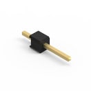 | WR-PHD Stiftleisten - Einreihig, 1, Gerade | Status Aktivi| Produktion ist aktiv. Erwartete Lebenszeit: >10 Jahre. | ProduktserieWR-PHD Stiftleisten - Einreihig | Pins1 | TypGerade | MontageartTHT | Länge2.54 mm | Nennstrom3 A | Arbeitsspannung250 V (AC) | Betriebstemperatur -40 °C up to +105 °C | |||
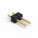 | WR-PHD Stiftleisten - Einreihig, 2, Gerade | Status Aktivi| Produktion ist aktiv. Erwartete Lebenszeit: >10 Jahre. | ProduktserieWR-PHD Stiftleisten - Einreihig | Pins2 | TypGerade | MontageartTHT | Länge5.08 mm | Nennstrom3 A | Arbeitsspannung250 V (AC) | Betriebstemperatur -40 °C up to +105 °C |