Texas Instruments TPS65090A
TPS65090 Front-End PMU With Switched-Mode Charger for 2 to 3 Cells In Series
Details
| Topologie | Abwärtswandler |
| Eingangsspannung | 6-17 V |
| Schaltfrequenz | 1360-1840 kHz |
| Ausgang 1 | 3.3 V / 5 A |
| Ausgang 2 | 5 V / 5 A |
| Ausgang 3 | 1.35 V / 5 A |
Beschreibung
The TPS65090A device is a single-chip power management IC for portable applications consisting of a battery charger with power path management for a dual or triple Li-Ion or Li-Polymer cell battery pack. The charger can be directly connected to an external wall adapter. Three highly efficient step-down converters are targeted for providing a fixed 5-V system voltage, a fixed 3.3-V system voltage, and an adjustable voltage rail. The step-down converters enter a low power mode at light load for maximum efficiency across the widest possible range of load currents. The step-down converters allow the use of small inductors and capacitors to achieve a small solution size. The TPS65090A also integrates two general-purpose always-on LDOs for powering circuit blocks which control the system while shut down. Each LDO operates with an input voltage range from 6 V to 17 V, allowing the LDOs to be supplied from the wall adapter or directly from the main battery pack.
Seven load switches are built into the device. These load switches can be used to control the power supply individually for certain circuit blocks in the application circuit. The current flowing through the load switches, as well as the output current of the step-down converters, the input current from the AC adapter and the charge current is monitored and can be read out using the digital interface.
For all available packages, see the orderable addendum at the end of the data sheet.
Eigenschaften
Wide Input Voltage Charger/Power Path Management:
VIN Range From 6 V to 17 V
– Up to 4 A Output Current on the Power Path
– Switchmode Charger; up to 4 A Maximum Charge Current
– JEITA Compliant Charging Control
– Thermal Regulation, Safety Timers
– 2 Temperature Sense Inputs
- 3 Step-Down Converters:
– High Efficiency over a wide Output Current Range
– VIN Range From 6 V to 17 V
– 2 Fixed Output Voltages ( 5 V and 3.3 V)
– 1 Adjustable Output Voltage (between 1.0V and 5.0V)
- Up to 4 A of Continuous Output Current
– Output Voltage Accuracy ±1%
– Typical 30 μA Quiescent Current per Converter
- 2 Always On LDO's:
– 2 Fixed Output Voltages ( 5 V and 3.3 V)
– Output Voltage Accuracy ±1%
– Typical 10 μA Quiescent Current per LDO
- 7 Current Limited Load Switches:
– One System Voltage Switch with 1 A Current Limit
– One 5 V Switch with 200 mA Current Limit, reverse voltage protected
– One 3.3 V Switch with 3 A Current Limit
– Four 3.3 V Switches with 1 A Current Limit
– All Switches Controlled by I2C Interface
- I2C Interface
– Standard-mode (100 kHz) supported
– Fast-mode (400 kHz) supported
– Fast-mode Plus (1000 kHz) supported
– High speed (3.4 MHz) supported
- 16 Channel 10 Bit A/D Converter
- Available in a 9 x 9-mm, VQFN-100 Package
Remarks:
- At the DC-DC converters, TI recommends using a 2.2-μH inductor with an appropriate current rating for theapplication.
- From Figure 3. TPS65090EVM Schematic Converters and Load Switches, J1 is for i/p, J4, J5, J6 is for o/p. see page num 3.
Typische Anwendungen
- Notebook Computer
- Mobile PC's and Mobile Internet Devices
- Battery Powered Products using 2 to 3 Li-Cells in Series
- Industrial Metering Equipment
- Personal Medical Products
Weiterführende Informationen
Artikeldaten
| Artikel Nr. | Datenblatt | Simulation | Downloads | Status | Produktserie | L (µH) | IRP,40K (A) | ISAT,10% (A) | ISAT,30% (A) | RDC max. (mΩ) | fres (MHz) | Montageart | Muster | |
|---|---|---|---|---|---|---|---|---|---|---|---|---|---|---|
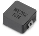 | 74437324022 | SPEC | 9 Dateien | Aktiv i| Produktion ist aktiv. Erwartete Lebenszeit: >10 Jahre. | WE-LHMI SMT Speicherdrossel | 2.2 | 4.05 | 4.45 | 8.4 | 61 | 49 | SMT |
| Artikel Nr. | Datenblatt | Simulation | |
|---|---|---|---|
 | 74437324022 | SPEC |
| Muster |
|---|
| Artikel Nr. | Datenblatt | Simulation | Downloads | Status | Produktserie | L (µH) | IRP,40K (A) | ISAT,10% (A) | ISAT,30% (A) | RDC max. (mΩ) | fres (MHz) | Montageart | Muster |
|---|


