Basic PCBs
Single-/double-sided and multilayer PCBs
Single-sided, double-sided and multilayer PCBs
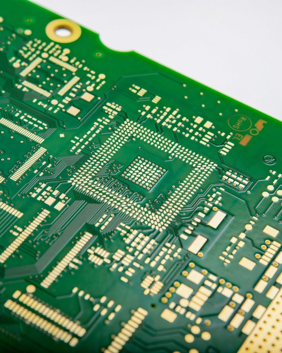
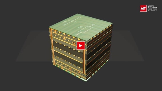
Under the term BASIC technology we combine single-sided, double-sided and multilayer printed circuit boards. Each PCB is something special, unique - your creation, made by us. Manufactured from base material in FR4 quality, this technology provides the reliable foundation for many applications, for example in industry, medical technology, automotive and aerospace.
With metallized through holes (PTH = plated through hole) as component holes and as electrical connection between the copper layers, it is possible to route a wide variety of electronic components up to a 0.8 mm pitch BGA. This makes your circuit plan and your individual solution a reality.
Good - better - standard: Standards are also the basis for quality and efficiency in the form of proven layer structures and design rules. Ensure error prevention and productivity increase in design, manufacturability as well as reliability of the PCB in the application.
Advantages of Würth Elektronik basic technology
We explain materials used and the basic process steps. Application examples illustrate the diverse fields of application of PCBs.
Relevant parameters for production-ready PCB design
Modern printed circuit board solutions are more than just connecting elements. They are the key to progress in electronics. With this in mind, we actively support our customers in their development and also offer our own system solutions with electronic functions.
In our BASIC design rules you will find all the parameters you should consider when designing and laying out printed circuit boards.
In addition, in the design guide "Plugging-Filling-Tenting", we have summarized not only basic definitions of terms, but also the individual designs of vias with their respective objectives in a clear manner for you. This will help you find the right solution for each of your use cases - within IPC-4761 and beyond.
Would you like to download our design guides and design rules as a clear technology poster? The poster provides you with the most important information about efficient PCB design.
Relevant parameters for production-optimized PCB design
Modern printed circuit board solutions are more than just connecting elements. They are the key to progress in electronics. With this in mind, we actively support our customers in the development and also offer our own system solutions with electronic functions.
In our BASIC design rules you will find all the parameters you should consider when designing and laying out PCBs.
In addition, in the design guide "Plugging-Filling-Tenting", we have summarized not only basic definitions of terms but also the individual versions of vias with their respective objectives. So you will find the right solution for each of your applications - within the IPC-4761 and beyond.
Get started with your layout faster - thanks to standardized layer stackups
With these stackups, you automatically use market-customary and cost-optimized standards and avoid expensive custom builds. In addition, high-quality and cost-effective production with shorter delivery times is made possible because stocked materials are used and standardized production processes are followed.
Our standards offer a base copper thickness of 18 µm or 35 µm on the inner layers. For fine structures and good manufacturability, 18 µm is preferred.
Here you can find our BASIC standard layer structures in digital form for import into your EDA software and as PDF:
The minimum structures have even improved in some cases, in no case have they worsened.
However, the derivation or presentation has changed:
Regarding the question it looks like this:
Inner layers can be structured simply by etching, the copper design is covered by resist for this purpose. In the process of outer layers, in addition to the pure structuring, the holes (PTHs) have to be metallized to establish the electrical connection between the copper layers. For this purpose, copper is deposited in the hole barrel and on the outer layers. For photo-structuring, the process must therefore be inverted, the holes and the copper design are open for copper buildup, and the resist prevents copper buildup in the places where there should be no copper in the end product.
This question is generally discussed very controversially, there are arguments for and against. From our experience, removal does not bring any significant improvements in terms of manufacturability and manufacturing costs. In addition, there is less anchoring and stability of the barrel, which can have a negative effect during thermo-mechanical stress, for example soldering cycles or temperature changes in field use. With RIGID.flex technology, the removal of non-used/non-functional pads on the polyimide layers must be avoided at all costs - otherwise reliability can be severely impaired!
Basically, in this 1 oz. to ½ oz. comparison (35 µm copper foil thickness to 17.5 µm), the thinner copper foil is less expensive. At the same time, smaller spacings are easier to produce with the thinner foil thickness, and the higher yield also has a cost-reducing effect.
The copper distribution should basically be as uniform as possible. For signal layers, the area share of copper is lower than for planes, but should be in the range of 40 to 60 %. Larger areas without copper should be filled and connected to a defined potential. For example, a high area copper content improves heat dissipation through heat distribution and heat dissipation. High uniformity of copper distribution is important for manufacturability with low thickness and etch tolerances and low board warpage.
IPC-2221 defines that the conductor width is measured at the base, see IPC-2221B Fig. 10.1. The manufacturing data for the photoresist are therefore modified accordingly with the aim of achieving the desired final width according to customer data after etching.
Prepreg (and copper foil) on the outside is easier and cheaper, the layer stack needs one core less. Prepreg and copper foil do not carry structures and therefore do not need to be registered to the inner layers. In the case of cores on the outside, their inner layers must be structured before pressing and registered for pressing, while the outer sides must remain completely covered with copper for the subsequent processes. The manufacturing process with foil lamination is therefore simpler than with core lamination.
Always the final diameter, only for press-fit holes the tool diameter is specified additionally.
With the standard process, the edge coverage is at least 5 µm. With multiple coating, the coating is thicker everywhere, and with s.mask technology, the coating thickness can be increased locally.
At Würth Elektronik, the material for prepregs and cores in one stackup is always of the same grade, i.e. BASIC Multilayer is made of FR4 from one manufacturer. The prepregs are made of the same material as the cores, but the resin is not fully cured ("B-stage"). As in the production of the core (from prepregs and copper foil), the prepreg resin is just fully cured (cross-linked, "C-stage") during multilayer production.
Yes, even then the conductors and copper structures should be protected from contact and contamination. So solder mask has a function not only for the soldering process, but also for the use of the PCB.
BASIC PCBs
We dive into the fascinating world of printed circuit boards and learn about BASIC technology. What are BASIC printed circuit boards made of? What is a multilayer? And how are the numerous layers, even if not 1,000, produced?
Our "Mr. Webinar" Andreas Schilpp answers the TOP 3 questions from the last 100 webinars in detail.
In our webinar we will offer you insights into:
The first of your top 3 webinars, originally offered in May 2013, is more relevant than ever. Recently, the Würth Elektronik BASIC Design Rules have been revised and restructured.
Did you know, for example, that for PCB manufacturing processes, the parameter "conductor width" is quite insignificant?
In this webinar you will learn more about
For example, did you know that switching to a slightly smaller drill bit can cause a much higher PCB price in some circumstances? The webinar will be of interest to developers, purchasing and management. Get insight into how PCB design is linked to the implications for PCB manufacturing and the costs involved. We provide guidance on the general cost structure of a PCB with a view to its layout and geometry.
The printed circuit board is generally underestimated. Functionally, it carries and connects electronic components and thus translates the electrical circuit diagram and its functions into hardware. It is thus increasingly becoming a strategically important component for the overall system itself.
Materially, the PCB is a very complex construct, manufactured by a multitude of sequential processes from a wide variety of materials, which must also be suitable for further processing and the intended application.
Understanding this helps in PCB design to be able to successfully implement the requirements from the functional specification in the design and the knowledge equally helps in communicating with the PCB manufacturer.
Contact us

