BASIC Physical PCB Sample WE.fan
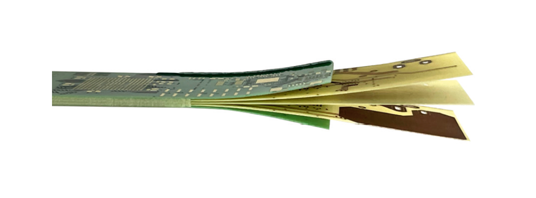
Our BASIC hand sample WE.fan shows you, partially pressed or fanned out, the basic structure of a multilayer with 6 copper layers in foil technology.
Two cores carry the inner layers and are visible in the fan (right). Top and bottom layout are on copper foils and pressed with the cores by means of prepreg to form the multilayer.
Electroless nickel/gold (ENIG) is used as the solder surface.
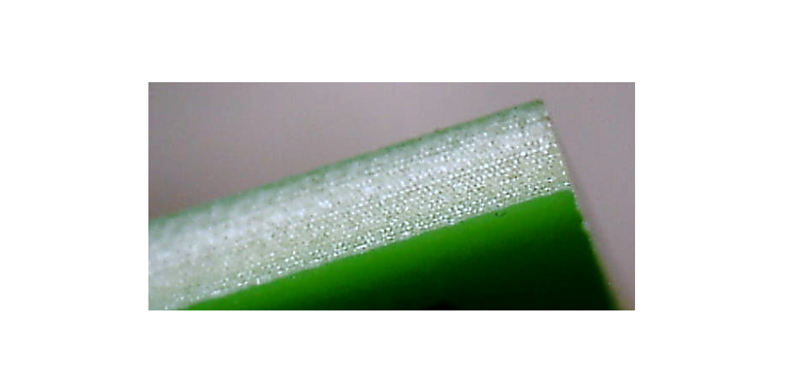
The contour is milled.
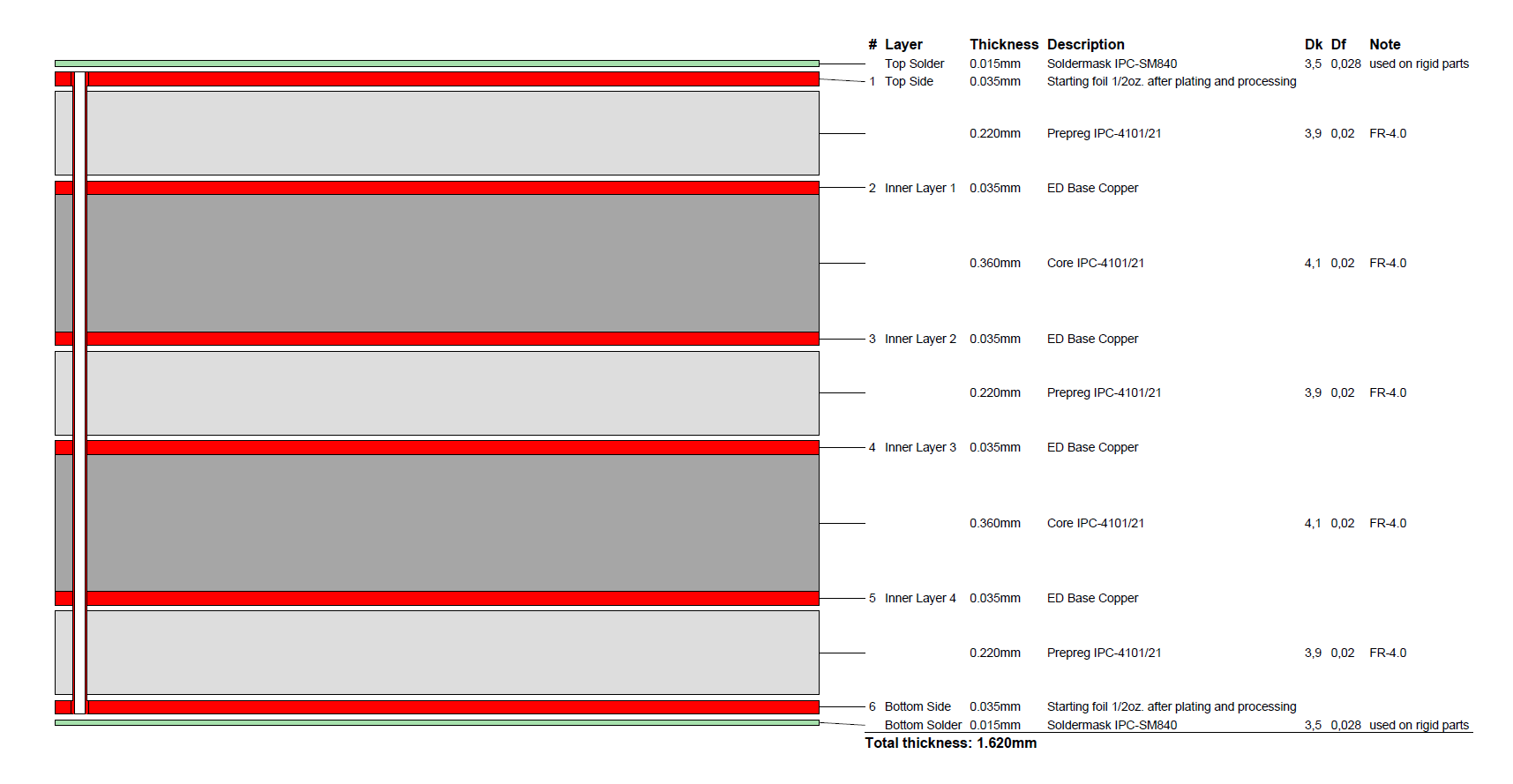
Stackup: BASIC6_ML6_1.62_35
Explanations: 6 copper layers with PTHs (Plated Through Holes), base material FR-4.0 Tg 135°, foil lamination with two cores, total thickness 1.62 mm, inner layer copper foil 35 µm (1 oz.).
Design: The multilayer is designed in three different parts.
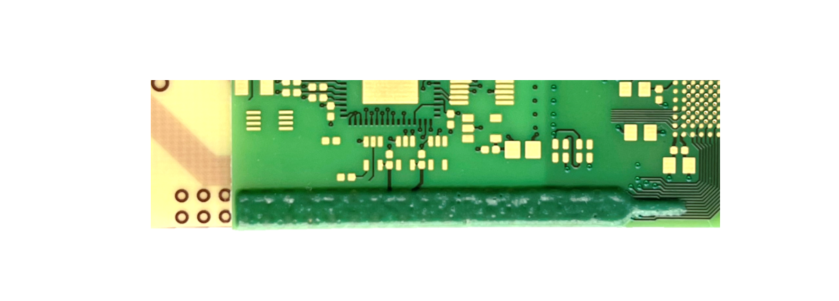
Explanation: Fully pressed and plated through in the left third, not pressed as a fan in the middle third with all layers, without outer layers in the fan on the right.
Design: The contour is milled
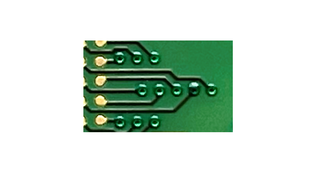
Design: One-sided plugging of the vias by plugging ink in silk screen printing
Explanations: Comparable to type IIIa according to IPC-4761, but plugging process after application of solder surface: The PTH barrel is completely coated with electroless nickel/gold for high reliability!
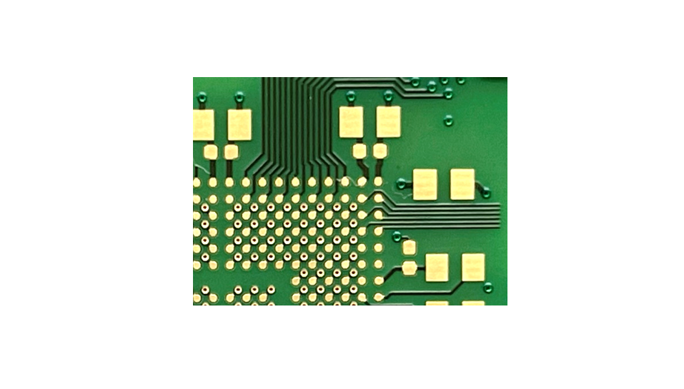
Design: Economical standard design rules with 6 mil (152 µm) spacing, standard PTHs with dog-bone connection
Design: In the connector area on top peelable solder mask, formed handling aid on the right
DESIGN: Insulation foil out of polyimide to provide secure insulation. Outline milled.
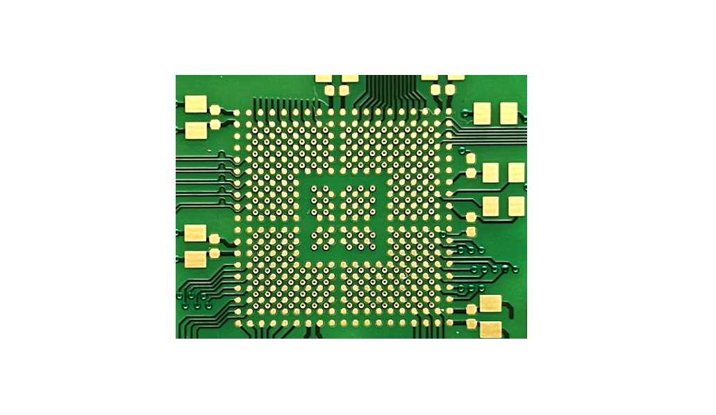
Design: The most complex component is a processor in BGA design with a pitch of 0.8 mm. This can just be routed without microvias. From a BGA pitch smaller than 0.8 mm, we recommend an HDI design with microvias.
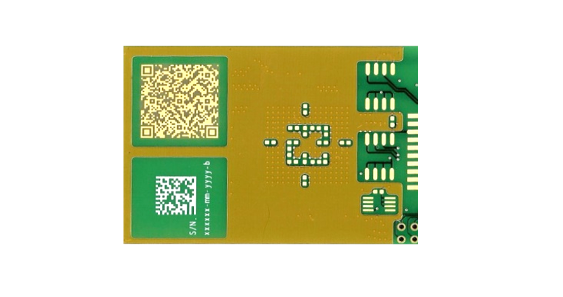
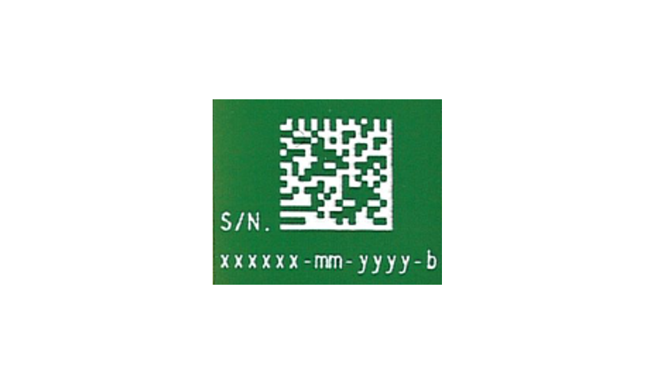
Explanation: execution in white lacquer by ink-jet, dynamic content is possible for singularization of any printed circuit board.
Design: link to this page via www.we-online.com/basicsample


