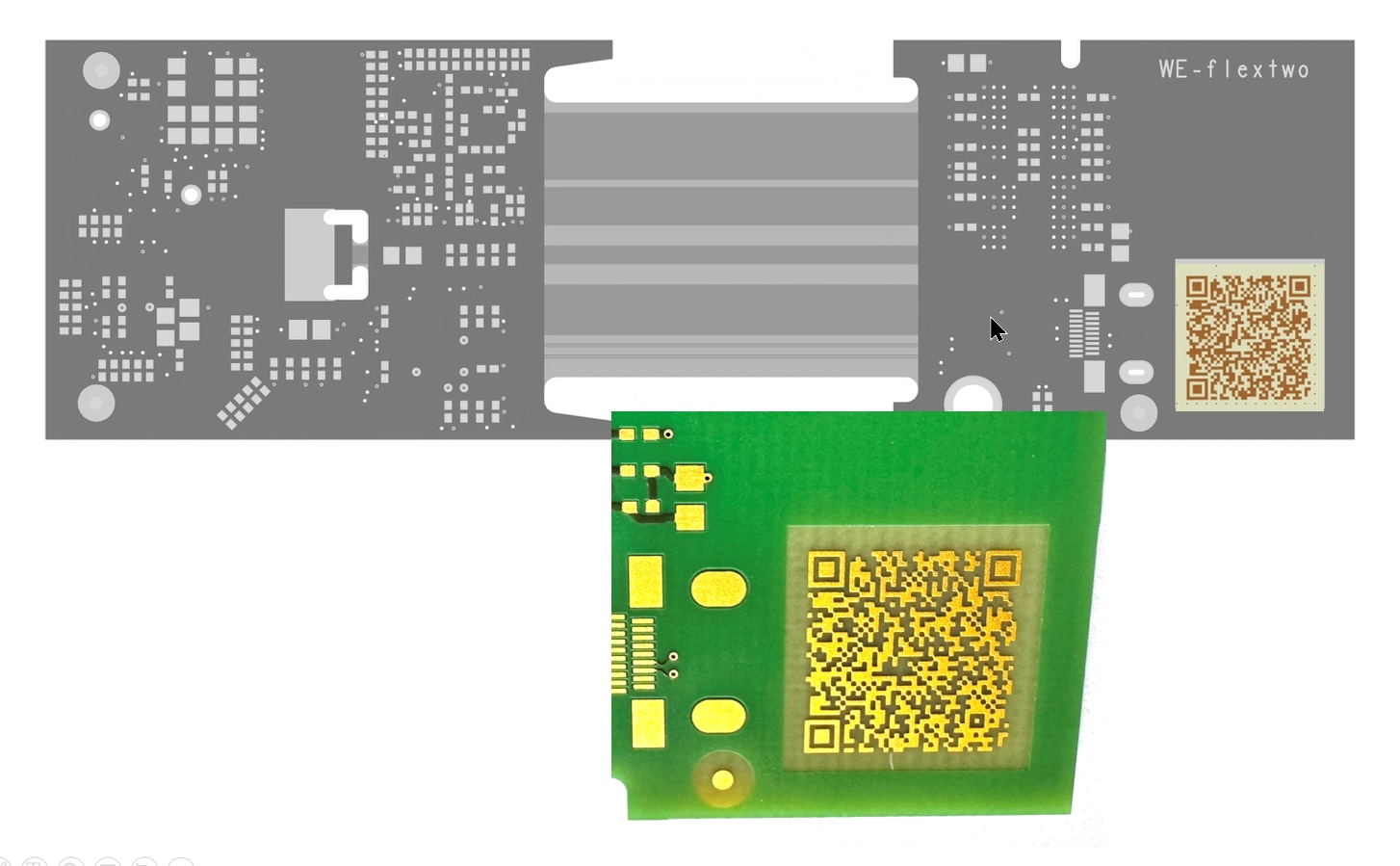
RIGID.FLEX Sample WE.flextwo
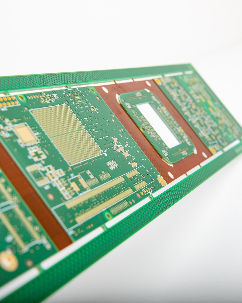
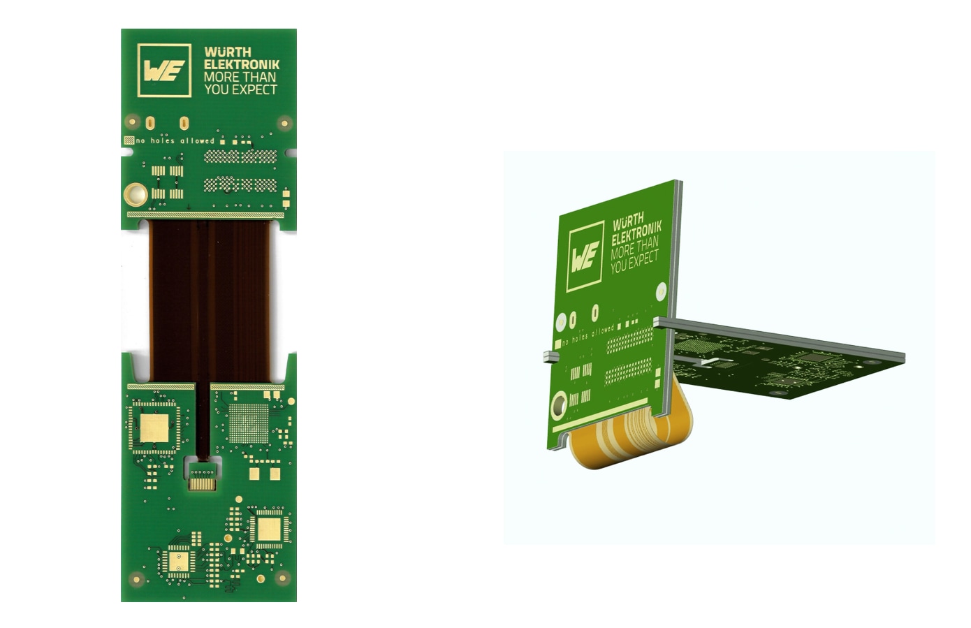
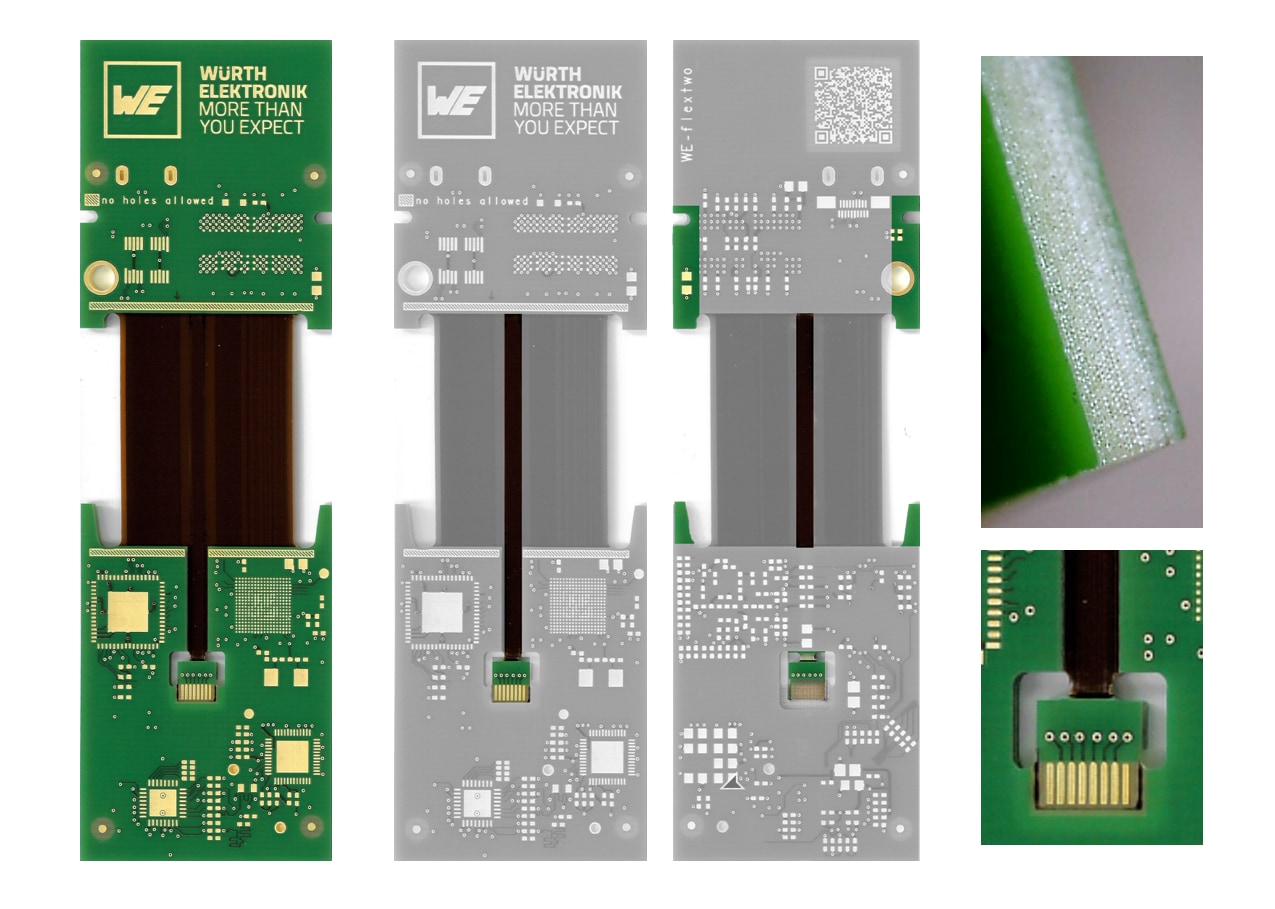
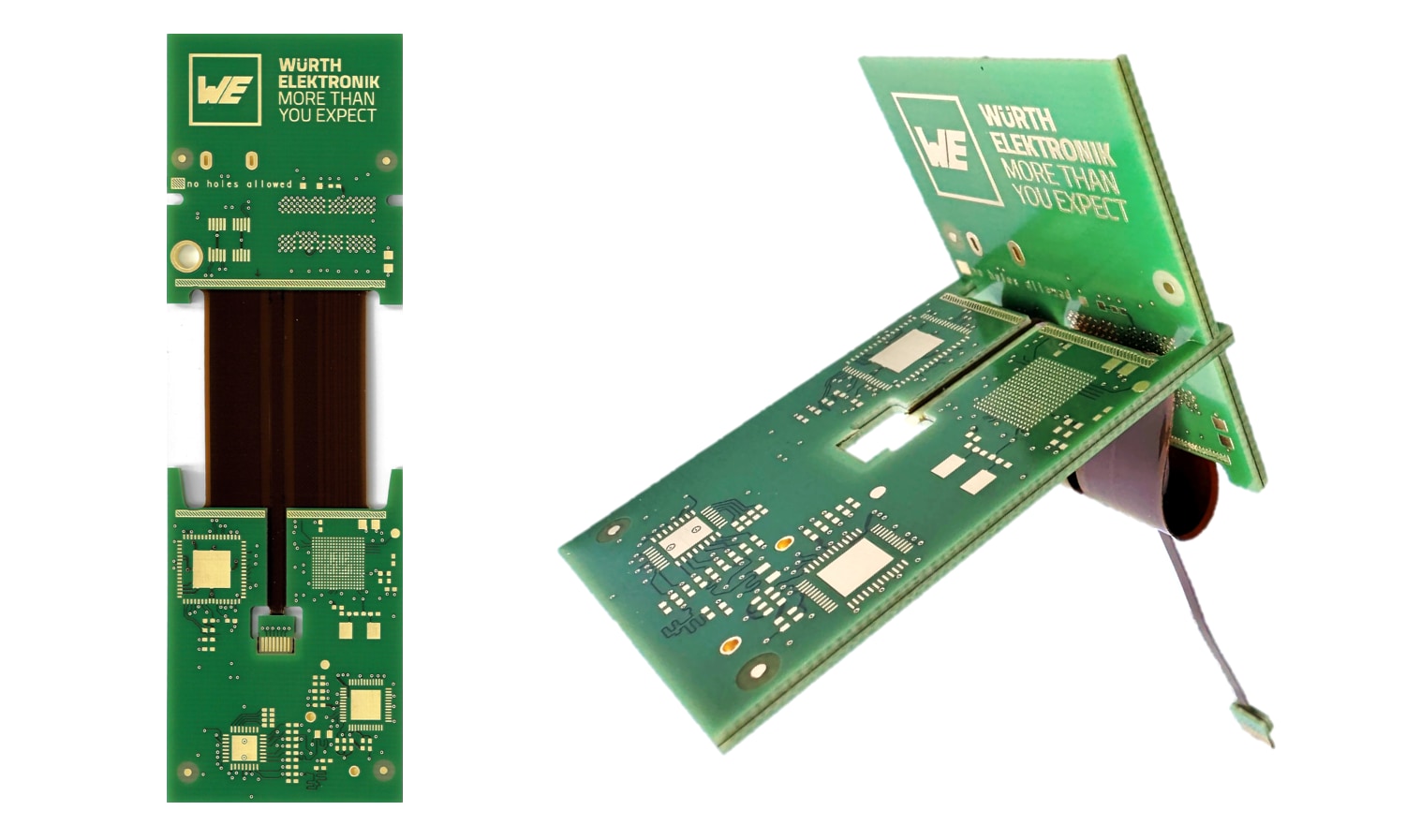
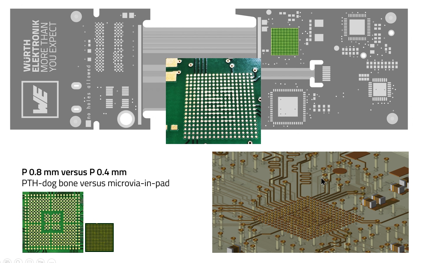
Our RIGID.flex physical sample WE.flextwo shows you the diverse mechatronic possibilities of this PCB technology with internal flex layers. Slot and key elements enable mechanical designs with options for fixing the rigid parts to each other. Non-glued lift-off areas and laser cuts offer a wide range of mechanical options for RIGID.flex technology. The use of microvias for unbundling a BGA with a pitch of 0.4 mm is indicated. The sample also shows an economically clever form of the popular ZIF contact with a layer change in the rigid area and contacts on the outer layer.
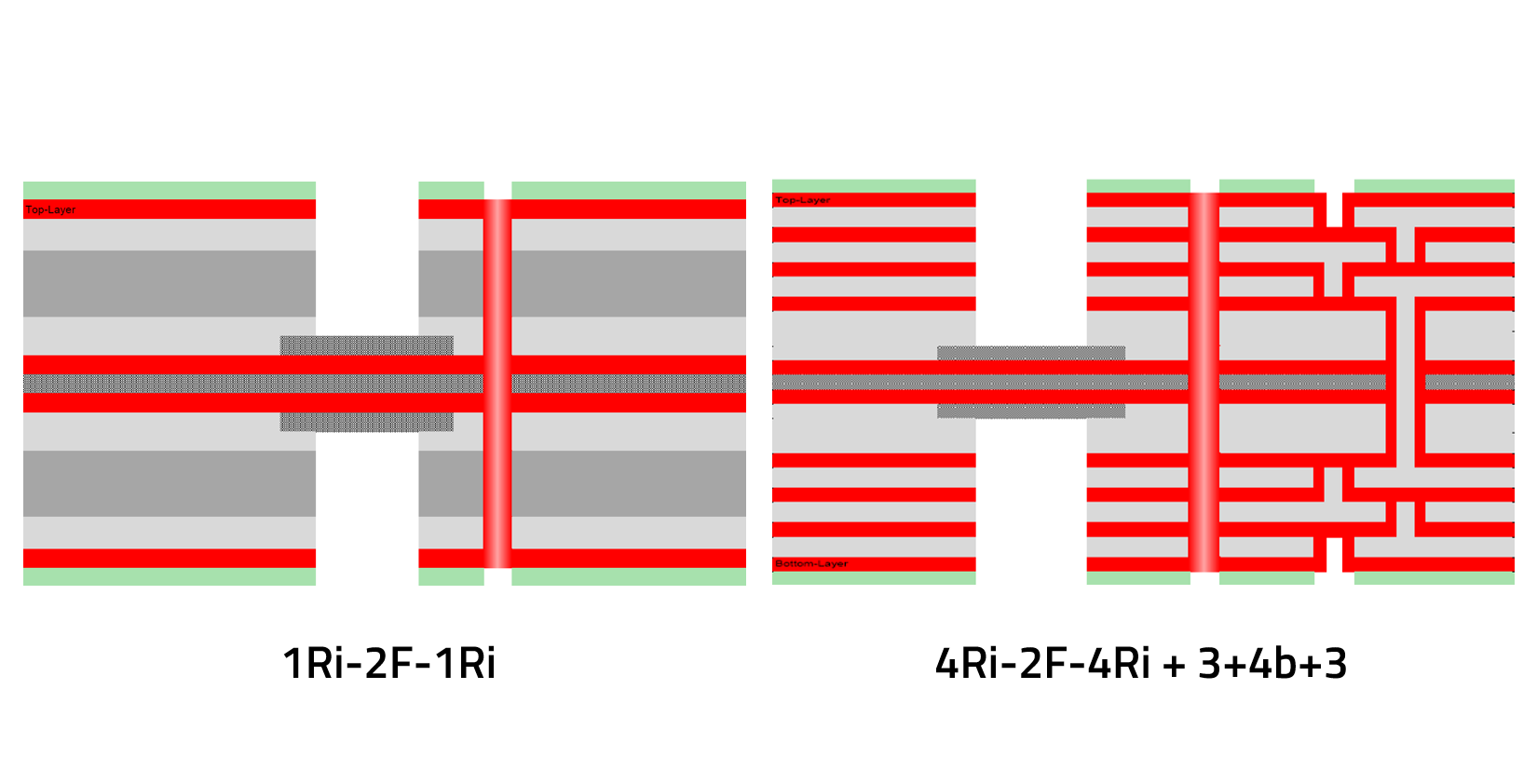
Design: Stackup: BEND.flex 2Ri-4Ri & SEMI.flex 1Ri-5Ri & SEMI.flex 2Ri-4Ri
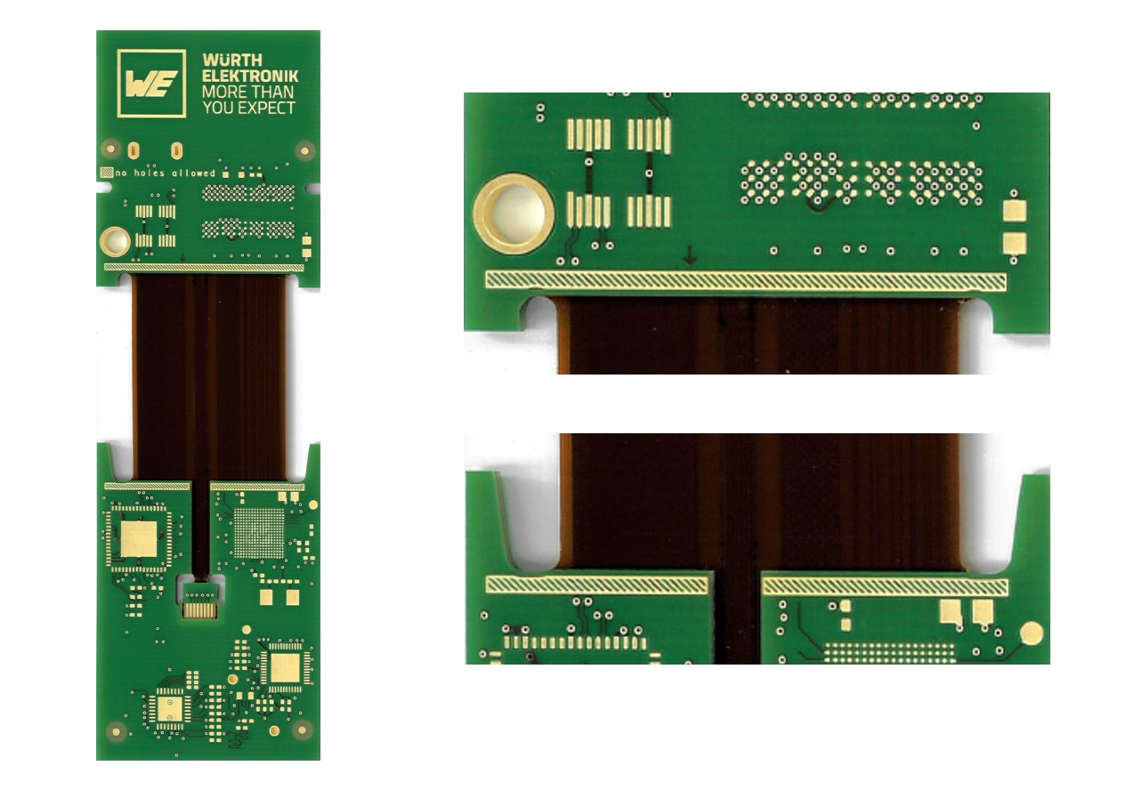
Explanations: The physical PCB sample shows bending areas with one and two copper layers. The bending areas are coated with flexible solder resist and their width is adapted to the permitted bending radii and bending angles.
Design: The outline of the physical PCB sample is milled. In compliance with the SEMI.flex design rules, a good SEMI.flex design has a recessed outline in the bending area with large radii in order to avoid notch effects during bending and thus achieve safe bending. A uniform bending moment by filling copper into copper-free surfaces is also important for uniform bending behavior.

