Slim.Flex – anylayer microvia technology that inspires
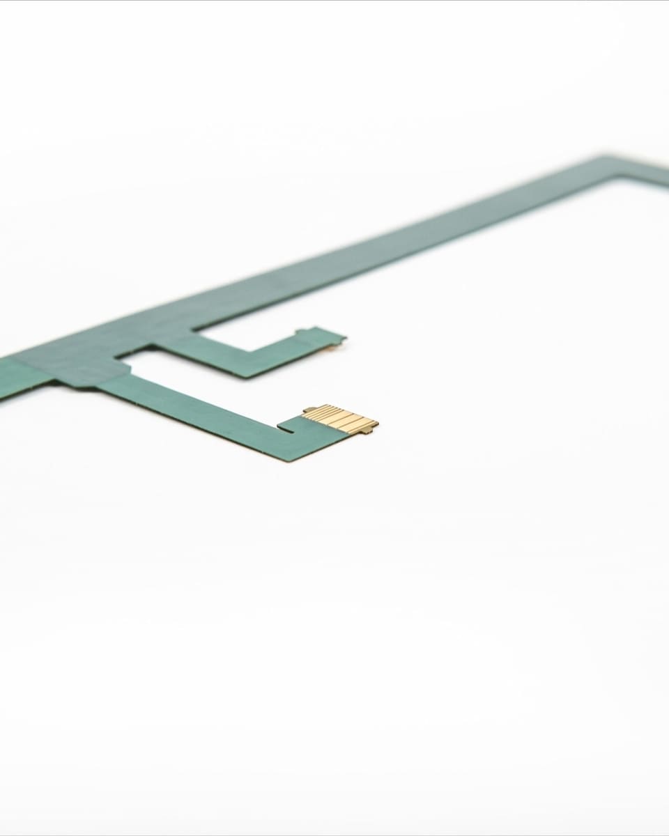
Small, compact, maximally bendable and highly resilient: These are the requirements for modern printed circuit boards. Whether for research or the medical, vision technology or automotive industries, SLIM.flex meets them with flying colors - even with the smallest housing volumes.
Wherever small and ultra-small sensors are required, the ultra-thin SLIM.flex products are convincing thanks to available standards as well as enormous robustness combined with maximum flexibility. Keyword flexible: This also applies to availability. From individual samples to series production, all variants can be ordered from the experts at Würth Elektronik.
Advantages of smart Würth Elektronik SLIM.flex technology
Application example
Intensive, verified quality tests have shown that SLIM.flex can withstand even the highest temperature stress and thus qualifies for use in highly demanding environments. The detectors of the world's largest particle accelerator, the LHC (Large Hadron Collider) at CERN in Geneva, rely on highly complex and ultra-thin HDI printed circuit boards from Würth Elektronik. Our SLIM.flex technology guarantees maximum reliability in the smallest possible installation space.
Features of the SLIM.flex PCBs in the LHC:
Technical details:
Application example
SLIM.flex technology allows ultra-dense, impedance-defined or shielded signals in the smallest possible space. Compared to conventional harnesses, this allows up to 100 percent more signals in half the installation space. Since there are no restrictions on signal routing and geometry in the design of the SLIM.flex harness, the harness can be designed in a very variable way.
Thanks to the universal layer structure, the number of flex layers can be changed as needed during layout without changing the stackup - and at no extra cost. By manufacturing the "harness" using PCB technology, wiring errors as with conventional harnesses can be eliminated. In addition, a reproducible, consistent arrangement of the signal routing is achieved.
The assembly time of the cable harness is drastically reduced by the use of preformed SLIM.flex, and ZIF contacts also eliminate the need to solder the cables or assemble connectors. A SLIM.flex cable harness can also be used as an integrated cable harness in applications with sensitive signals, for example for the smallest image sensors in endoscopes.
Technical details
Our customers benefit from state-of-the-art technology
Application analysis: HEINE DELTA 30 PRO dermatoscope
The HEINE DELTA 30 PRO dermatoscope is a medical examination instrument that impresses with its innovative arrangement of LEDHQ elements. This unique technology allows the light to reach deeper layers of the skin, creating an extremely vivid, spatial impression of lesions - comparable to a 3D image.
Technical details of the dermatoscope:
Success story of the DELTA 30 PRO dermatoscope project
The SLIM.flex technology proved to be the ideal solution for the customer HEINE Optotechnik GmbH & Co. KG , as a flat circuit board with a tight bending radius was required. Other suppliers were unable to meet these requirements either because the PCBs were too thick or the bending radius was too large.
In close cooperation between HEINE Optotechnik and Würth Elektronik, the minimum bending radii and bending directions of the SLIM.flex were determined, a suitable solder carrier was defined and the panel connection was designed. This cooperation made it possible to reduce the number of copper layers from 6 to 4, which resulted in both material and cost savings.
In addition, HEINE Optotechnik received comprehensive support during the introduction into series production.
Discover the advantages of SLIM.flex technology
Würth Elektronik's SLIM.flex technology offers innovative solutions for demanding applications where a flat PCB with a tight bending radius is required. Find out more about how our technology can help you to realize your projects efficiently and cost-effectively. Get in touch with us directly.
Relevant parameters for production-ready PCB design
Modern printed circuit board solutions are more than just connecting elements. They are the key to progress in electronics. With this in mind, we actively support our customers in development and also offer our own system solutions with electronic functions.
The SLIM.flex design rules include all the important parameters you need to make your project successful:
In our design guide you will find an overview of all variants of our flex solutions. In addition, our specialists have summarized valuable design tips for you here. This will help you bring your application to success reliably and safely.
Get started with your layout faster - thanks to standardized stackups
With these stackups, you automatically use market-customary and cost-optimized standards and avoid expensive special setups. They also enable high-quality, cost-effective production with shorter lead times by using stock materials and following standardized production processes.
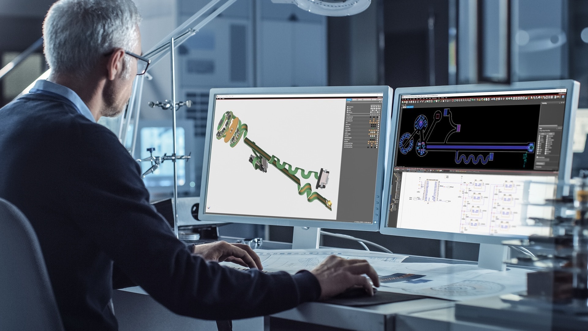
Here you can find our SLIM.flex standard stackups both in digital form for import into your EDA software, and as PDFs. The digital stackup files for Altium Designer contain not only the stackup but also the material data.
The SLIM.flex technology is designed for high wiring density. For this reason, the smallest vias in the form of laser-drilled microvias are used as a matter of principle. PTHs would be technically possible, but would then lead to higher copper layers and the loss of the finest structures.
Depending on the number of copper layers, the standard stackups have a thickness between 0.25 mm for 4 layers and 0.46 mm for 8 layers. Locally higher thicknesses can be achieved by stiffeners.
There are several possibilities for assembling SLIM.flex:
Würth Elektronik can supply your SLIM.flex PCB with an FR4 solder carrier, so that assembly is possible on normal automatic machines. In this case, only the array frame can be glued to the solder carrier, so that the PCB is fully flexible again after it has been removed from the frame.
A typical solder carrier is made of FR4 with a material thickness of 0.80 mm. This gives a total thickness with solder carrier of 1.0 mm for a SLIM.flex 4F-Ri. In the area of the solder carrier, backside assembly is not possible.
Yes, definitely. The advantage is that the thin stackups have only a very small expansion in Z-axis! Tests have shown that even under extreme conditions the circuits are extremely reliable.
In addition to quick samples, we also supply series, gladly also in larger quantities.
Understand Würth Elektronik SLIM.flex technology playfully
Learn in detail about the possibilities of SLIM.flex technology in terms of design and applications. The WE.scope hand sample shows the practical implementation of a vision concept from the sensor with illumination and cable harness to the coax connector - and all this in the smallest possible space. This hand sample is available both as a physical PCB sample and as a digital hand sample.
"More powerful than ever - the new SLIM.flex technology"
Ultra-thin. Rugged. Flexible like never before. And on top of that: Available with standards and digital stackups. That is SLIM.flex. The WE Circuit Board Technology PCB of the latest generation.
Find out in our webinar how you can benefit from SLIM.flex and from our competent expert advice as well as a complete delivery process of the PCB from a single source.
"Miniaturization, mechatronics, microvia: SLIM.flex physical PCB sample WE.scope!"
Find out more about SLIM.flex, our anylayer microvia flex technology. Wherever small and ultra-small components are used, such as sensors in micro-packages, the ultra-thin SLIM.flex products impress thanks to the available standards and enormous robustness combined with maximum flexibility. In this webinar we will offer you insights into our hand sample WE.scope and what you can learn from it.


