IC-Hersteller (96)
- Alle Hersteller
 Analog Devices
 Infineon Technologies
 Maxim Integrated
 Microchip
 Onsemi
 Renesas
 ROHM
ROHM STMicroelectronics
 Texas Instruments
- 3peak incorporated (12)
- Ablic (23)
- Advanced Power (4)
- Allegro Microsystems (83)
- Alpha & Omega Semiconductor (37)
- AnalogySemi (3)
- AnDAPT Inc (139)
- Anpec (13)
- AXElite (2)
- Backward (6)
- Broadcom (47)
- Cambridge GaN Devices (17)
- Chipanalog Micro (10)
- Cologne Chips (1)
- Dialog Semiconductor (11)
- Diodes Incorporated (219)
- Divimath (8)
- Elmos AG (1)
- EPC (98)
- e-Peas Semiconductors (1)
- Eta Solutions Co. Ltd. (9)
- GaN Systems (6)
- Giantec (1)
- Gstek Wuxi (1)
- Helix Semiconductor (7)
- Ikanos (3)
- IKON (1)
- Indie Semiconductor (2)
- Innovision Semiconductor Inc (2)
- Intel (80)
- Inventchip Technology (3)
- ISSI (36)
- JoulWatt (20)
- KDPOF (2)
- Kinetic Technology (9)
- Lattice semiconductor Corporation (19)
- Littelfuse (1)
- M3 Technology (M3Tek) (4)
- Macnica (16)
- MaxLinear (175)
- MikroE (8)
- MindCet (1)
- Monolithic Power Systems (899)
- Navitas Semiconductor Inc (6)
- NewEdge Technologies, Inc. (1)
- Nexperia (2)
- Nisshinbo Micro Device Inc. (10)
- Nordic Semiconductor (1)
- Novosense Micro (1)
- NXP (313)
- O2 Micro International Ltd (10)
- On Bright (7)
- Panasonic (2)
- PN Junction Semiconductor (2)
- Power Integrations (96)
- Pulsiv (18)
- Qorvo (87)
- Realsil SuRealsil(tek) Microelectronics (1)
- Richtek (292)
- Sanken Electric Co., Ltd. (16)
- Sckipio (6)
- Semtech (90)
- SG-Micro (20)
- Silanna Semiconductor (8)
- Silergy Corporation (29)
- Silicon Laboratory Inc. (90)
- Silicontent Technology (56)
- Silvertel (56)
- Skyworks (31)
- Southchip (8)
- Summit Wireless (1)
- Tagore Tech (7)
- Taiwan Semiconductor (1)
- TDK Corporation (1)
- Tempo Semiconductor (1)
- Torex (37)
- Toshiba (25)
- Transphorm (21)
- TransSIP (2)
- Union (21)
- uPI Semiconductor (1)
- Valens Semiconductor (18)
- Wise Integration (1)
- Wolfspeed (5)
- Xilinx (18)
- XL Semiconductor (3)
- XYSemi (62)
Details
| Topologie | Gegentaktwandler (Halbbrücken) |
| Eingangsspannung | 100 V |
| Schaltfrequenz | 100-10000 kHz |
| Ausgang 1 | 100 V |
Beschreibung
The LT8418 is a 100V half-bridge GaN driver that integrates top and bottom driver stages, driver logic control, and protections. It can be configured into synchronous half-bridge, full-bridge topologies, or buck, boost, and buck-boost topologies. The LT8418 provides strong current sourcing/sinking capability with 0.6Ω pull-up and 0.2Ω pull-down resistance. It also integrates smart integrated bootstrap switch to generate a balanced bootstrap voltage from VCC with a minimum dropout voltage.The LT8418 provides split gate drivers to adjust the turn-on and turn-off slew rates of GaN FETs to suppress ringing and optimize EMI performance. All driver inputs and outputs have default low-state to prevent GaN FETs from false turn-on. The inputs of the LT8418, INT, and INB are independent and TTL logic compatible. Meanwhile, the LT8418 performs with a fast propagation delay of 10ns and maintains an excellent delay matching of 1.5ns between the top and bottom channels, making it suitable for high-frequency DC-DC converters, motor drivers, and class-D audio amplifiers. In addition, the LT8418 employs the WLCSP package to minimize parasitic inductance, enabling its wide use in high-performance and high-power density applications.
Eigenschaften
- Half-Bridge Gate Driver for GaN FETs
- 0.6Ω Pull-Up Resistance at Top Gate Driver
- 0.2Ω Pull-Down Resistance at Bottom Gate Driver
- 4A Peak Source, 8A Peak Sink Current Capability
- Smart Integrated Bootstrap Switch
- Split-Gate-Driver to Adjust Turn-On/Turn-Off Strength
- Default Low-State for All Driver Inputs and Outputs
- Maximum 15V Voltage Rating at INT and INB Inputs
- Independent INT, INB Inputs with TTL Logic Compatible
- Fast Propagation Delay: 10ns (Typical)
- Propagation Delay Matching: 1.5ns (Typical)
- Balanced Driver Supply Voltage: VBST ≈ VCC = 3.85V – 5.5V
- Undervoltage and Overvoltage Lockout ProtectionsSmall 12-Ball WLCSP Package
Typische Anwendungen
Weiterführende Informationen
Artikeldaten
| Artikel Nr. | Datenblatt | Simulation | Downloads | Produktserie | L (µH) | IRP,40K (A) | ISAT1 (A) | ISAT,30% (A) | RDC max. (mΩ) | fres (MHz) | Muster | |
|---|---|---|---|---|---|---|---|---|---|---|---|---|
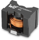 | 7443630310 | SPEC | 8 Dateien | WE-HCF SMT-Hochstrominduktivität | 3.1 | 33.15 | 41 | 45 | 2.3 | 29 |
| Artikel Nr. | Datenblatt | Simulation | |
|---|---|---|---|
| 7443630310 | SPEC |
| Muster |
|---|
| Artikel Nr. | Datenblatt | Simulation | Downloads | Produktserie | L (µH) | IRP,40K (A) | ISAT1 (A) | ISAT,30% (A) | RDC max. (mΩ) | fres (MHz) | Muster |
|---|