IC-Hersteller Texas Instruments
IC-Hersteller (104)
- Alle Hersteller
 Analog Devices
 Infineon Technologies
 Microchip
 Onsemi
 Renesas
 ROHM
ROHM STMicroelectronics
 Texas Instruments
- 3peak incorporated (28)
- Ablic (23)
- Acco Semiconductor (1)
- Advanced Power (4)
- Allegro Microsystems (97)
- Alpha & Omega Semiconductor (37)
- AnalogySemi (3)
- AnDAPT Inc (204)
- Anpec (13)
- AXElite (2)
- Backward (6)
- Bright Power Semiconductor (1)
- Broadcom (45)
- Cambridge GaN Devices (18)
- Chipanalog Micro (10)
- Cologne Chips (1)
- Convenient Power (1)
- Dialog Semiconductor (12)
- Diodes Incorporated (255)
- Divimath (8)
- Elmos AG (1)
- EPC (135)
- e-Peas Semiconductors (1)
- Eta Solutions Co. Ltd. (9)
- GaN Systems (8)
- GaNPower (3)
- Giantec (1)
- Gstek Wuxi (1)
- Helix Semiconductor (7)
- IKON (1)
- Indie Semiconductor (8)
- Innovision Semiconductor Inc (2)
- Intel (68)
- Inventchip Technology (3)
- ISSI (51)
- JoulWatt (20)
- KDPOF (3)
- Kinetic Technology (8)
- Lattice semiconductor Corporation (30)
- Littelfuse (1)
- Lumissil Microsystems (8)
- M3 Technology (M3Tek) (7)
- Macnica (22)
- Marvell Semiconductor (1)
- MaxLinear (181)
- Menlo Micro (1)
- MikroE (21)
- MindCet (2)
- Monolithic Power Systems (979)
- Navitas Semiconductor Inc (6)
- NewEdge Technologies, Inc. (1)
- Nexperia (263)
- Nisshinbo Micro Device Inc. (10)
- Nordic Semiconductor (1)
- Novosense Micro (1)
- NXP (327)
- O2 Micro International Ltd (10)
- On Bright (7)
- Panasonic (2)
- PN Junction Semiconductor (2)
- Power Integrations (120)
- Powermat (1)
- Pulsiv (19)
- Qorvo (95)
- Realsil SuRealsil(tek) Microelectronics (1)
- Richtek (297)
- Sanken Electric Co., Ltd. (16)
- Sckipio (6)
- Semtech (87)
- SG-Micro (49)
- SiFive (2)
- Silanna Semiconductor (9)
- Silergy Corporation (33)
- Silicon Laboratory Inc. (103)
- Silicontent Technology (59)
- Silvertel (61)
- Skycore Semiconductors (1)
- Skyworks (33)
- Southchip (8)
- Summit Wireless (1)
- Tagore Tech (7)
- Taiwan Semiconductor (1)
- TDK Corporation (1)
- Tempo Semiconductor (1)
- Torex (37)
- Toshiba (25)
- Transphorm (21)
- TransSIP (2)
- Union (21)
- uPI Semiconductor (2)
- Valens Semiconductor (30)
- Wise Integration (1)
- Wolfspeed (23)
- Xilinx (22)
- XL Semiconductor (3)
- XYSemi (62)
Texas Instruments LM26400YSDE | Demoboard TIDA-00432
Synchronization of JESD204B Giga-Sample ADCs using Xilinx Platform for Phased Array Radar Systems
Details
| Topologie | Abwärtswandler |
| Eingangsspannung | 12 V |
| Ausgang 1 | 1.2 V |
| IC-Revision | A |
Beschreibung
This system level design shows how two ADC12J4000 evaluation modules (EVMs) can be synchronized together using a Xilinx VC707 platform. The design document describes the required hardware modifications and device configurations, including the clocking scheme. Example configuration files are shown for each EVM. The FPGA firmware is described and the relevant Xilinx IP block configuration parameters are shown. Data taken on the actual hardware is shown and analyzed, showing synchronization within 50 ps without characterized cables or calibrated propagation delays.
Eigenschaften
- Demonstrates a typical phased array radar sub-system by showing synchronization of JESD204B giga-sample ADCs
- The LMK04828 clocking solution used is described in detail
- Test results show synchronization within 50 ps without any characterization of cables or calibration of propagation delays
- Xilinx firmware development is discussed to offer a clear understanding of the requirements
- This sub-system is tested and includes example configuration files
Typische Anwendungen
- Signal Measurement - Oscilloscopes
Weiterführende Informationen
Artikeldaten
| Artikel Nr. | Datenblatt | Simulation | Downloads | Status | Produktserie | L (µH) | IRP,40K (A) | ISAT,10% (A) | ISAT,30% (A) | RDC (mΩ) | fres (MHz) | Material | Muster | |
|---|---|---|---|---|---|---|---|---|---|---|---|---|---|---|
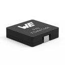 | 744325550 | SPEC | 9 Dateien | Aktiv i| Produktion ist aktiv. Erwartete Lebenszeit: >10 Jahre. | WE-HCI SMT-Hochstrominduktivität | 5.5 | 12 | 4.5 | 12 | 10.3 | 30 | Superflux |
| Muster |
|---|
| Artikel Nr. | Datenblatt | Simulation | Downloads | Status | Produktserie | L (µH) | IRP,40K (A) | ISAT,10% (A) | ISAT,30% (A) | RDC (mΩ) | fres (MHz) | Material | Muster |
|---|
