BEND.FLEX & SEMI.flex physical PCB sample WE.bend
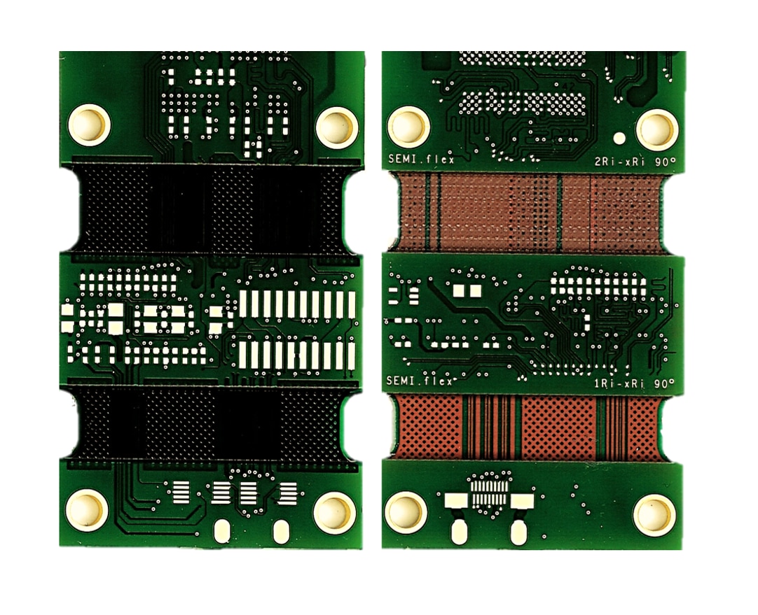
Our combined WE.bend physical PCB sample shows you a combination of the SEMI.flex and BEND.flex technologies and thus enables a direct comparison of the two variants. Feel the differences in bending performance in the truest sense of the word. This will help you understand the advantages and recognize the possible applications.
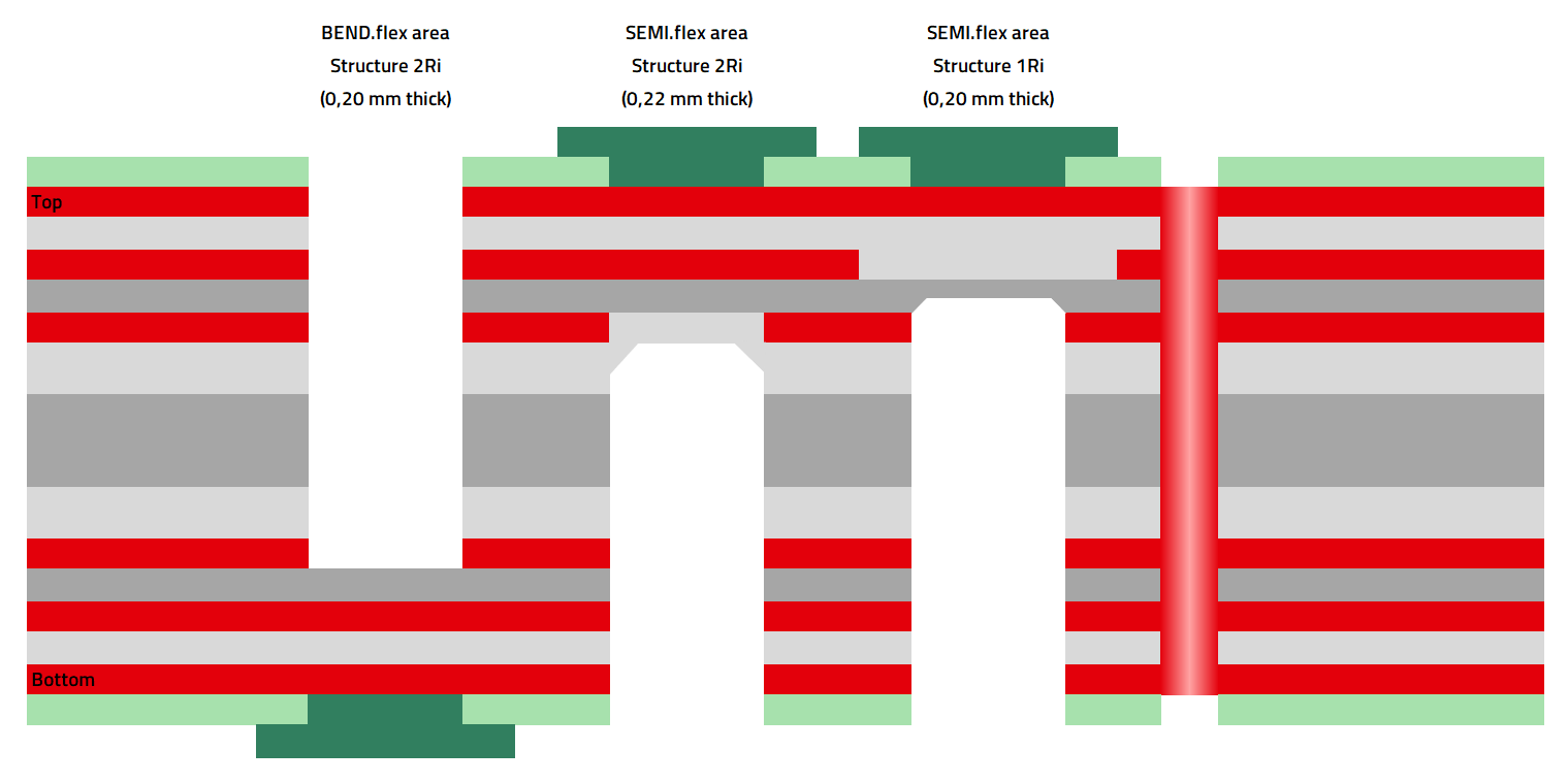
Design: Stackup: BEND.flex 2Ri-4Ri & SEMI.flex 1Ri-5Ri & SEMI.flex 2Ri-4Ri
Explanations: The physical PCB sample shows bending areas with one and two copper layers. The bending areas are coated with flexible solder resist and their width is adapted to the permitted bending radii and bending angles.
Design: The outline of the physical PCB sample is milled. In compliance with the SEMI.flex design rules, a good SEMI.flex design has a recessed outline in the bending area with large radii in order to avoid notch effects during bending and thus achieve safe bending. A uniform bending moment by filling copper into copper-free surfaces is also important for uniform bending behavior.
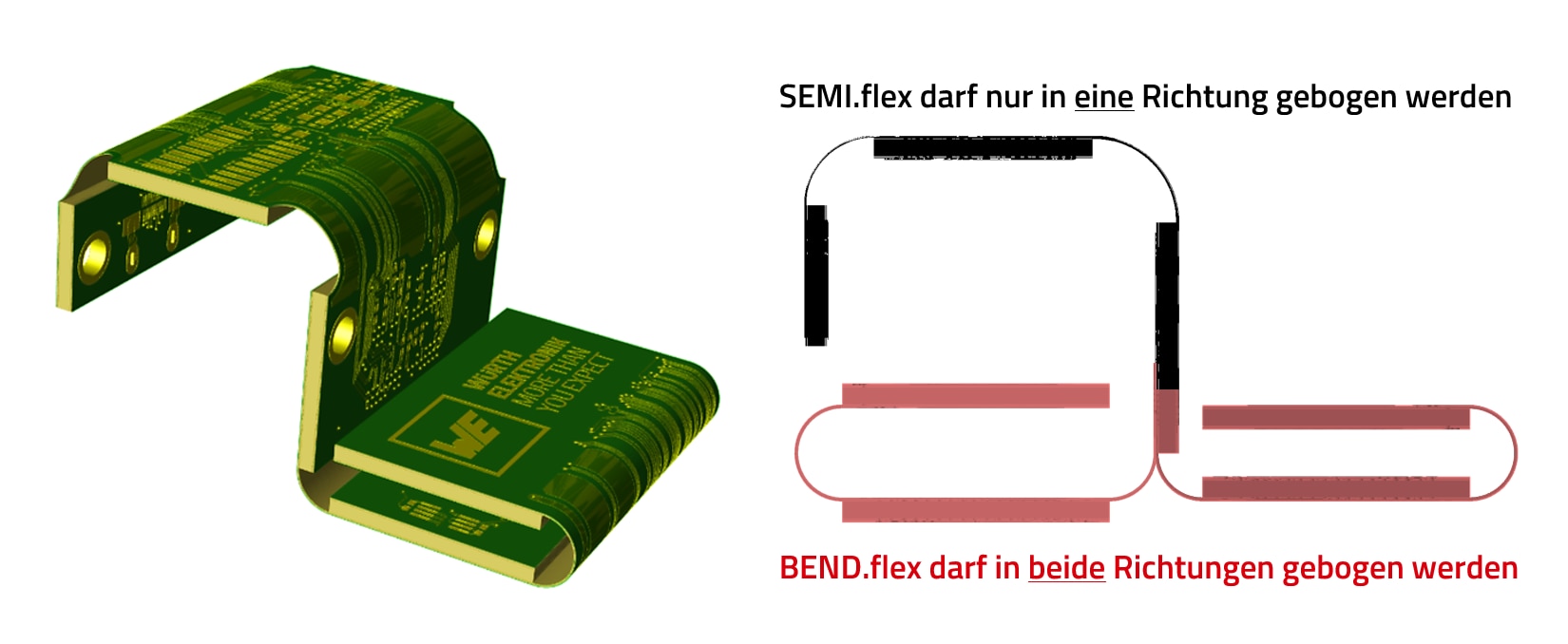
Design: Two three-dimensional configurations are possible with the physical PCB sample.
Explanations: While the SEMI.flex area may only be bent in one direction, bending in both directions is permitted with BEND.flex. The design rules allow a maximum bending angle of 90° for SEMI.flex and 180° for BEND.flex. SEMI.flex is more suitable for short bending ranges, BEND.flex can also be bent evenly with large bending areas.
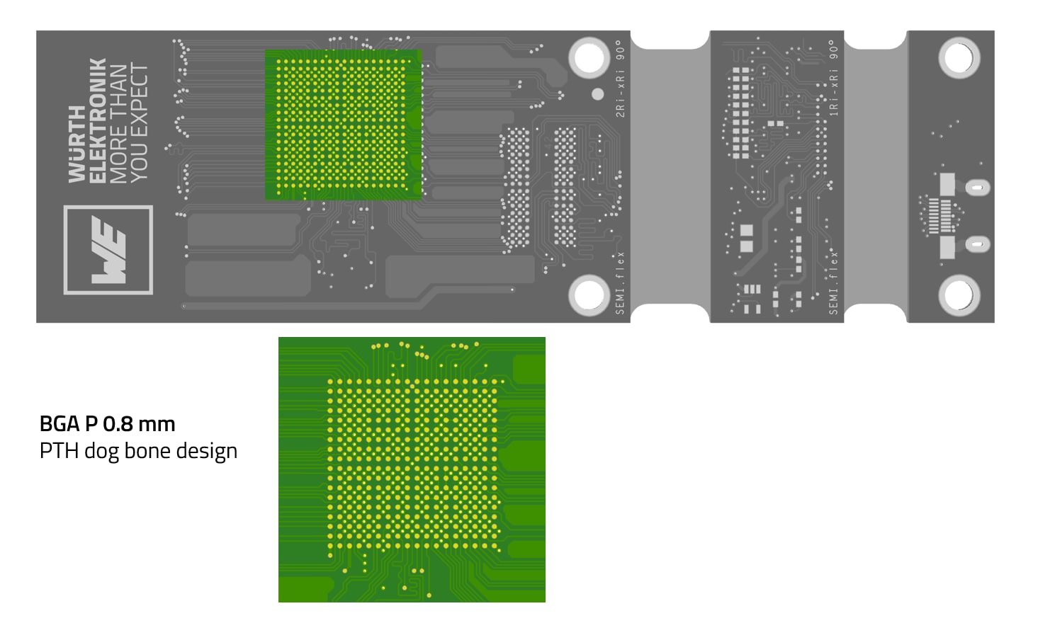
Design: The most complex component is a processor in BGA design with a pitch of 0.8 mm. This can just be routed without microvias. From a BGA pitch smaller than 0.8 mm, we recommend an HDI design with microvias.


