SLIM.flex Physical PCB Sample WE.scope
Our SLIM.flex physical PCB sample WE.scope shows you on the top:
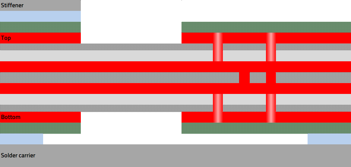
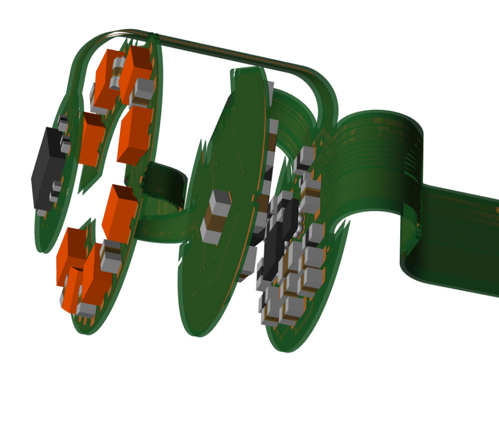
Space-saving mechatronic design, glued-on stiffener for a quasi-rigid part.
... and on the bottom:
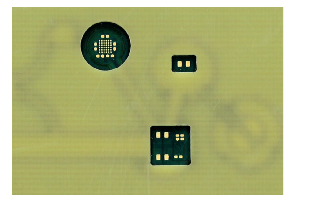
Solder carrier with cutouts for component placement. Holes in the solder carrier for easy detaching the SLIM.flex PCB assembled.
Stackup: SLIM.flex Ri-4F-Ri
Explanations: Anylayer microvia, thin, robust, impedance defined.
The solder carrier enables assembly and soldering using standard processes, and the assembled SLIM.flex PCB can be easily separated from the solder carrier.
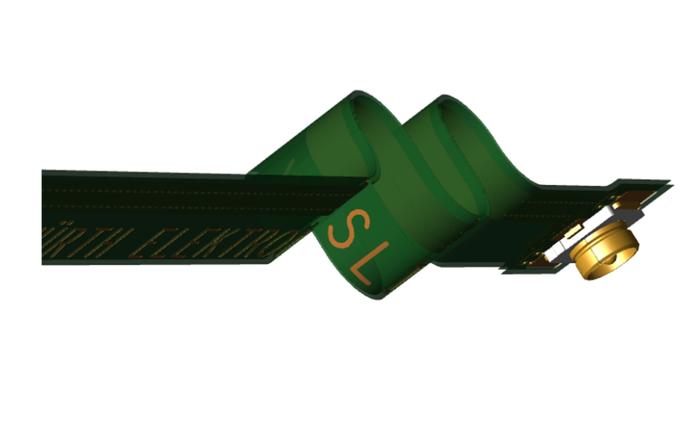
Design: planar/spatial
Explanation: Space-saving spatial arrangement, minimization of space requirements in planar manufacturing and placement state. Stiffener in the sensor area for reinforcement.
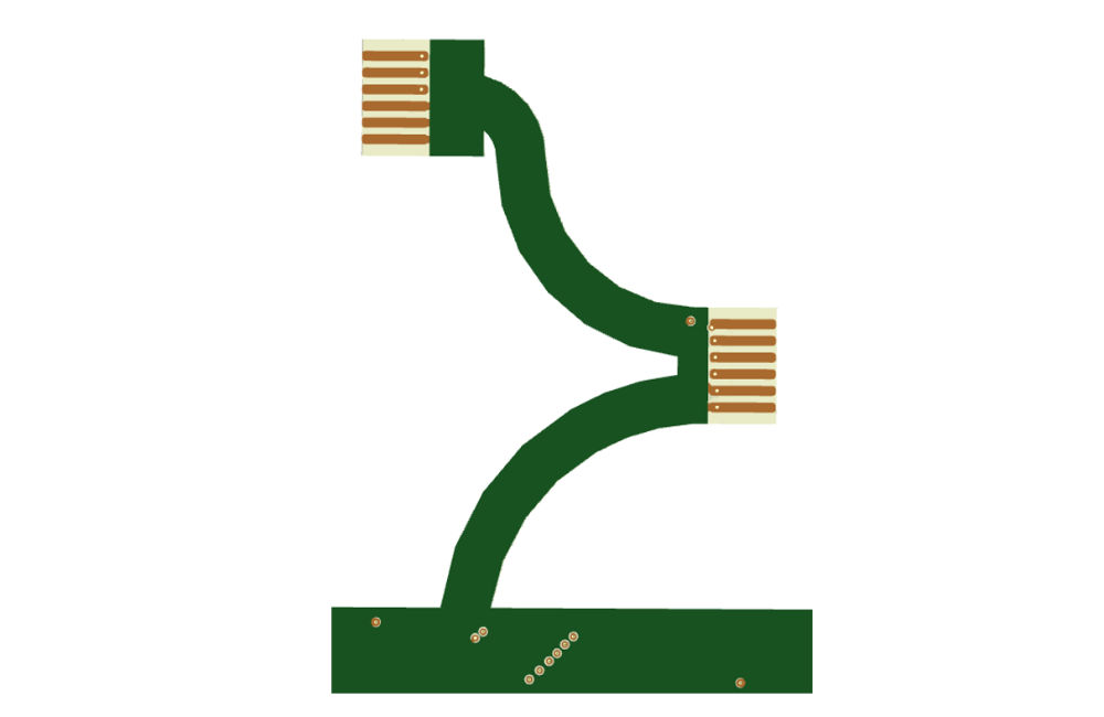
Design: Lasered, with micro webs
Design: Components on the back
Explanations: Placement in the cavity with a 3D step template, alternatively dispensing or Jetprint
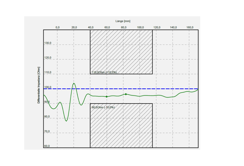
Design: Impedance models available. Please get in touch with us!
Fig.1
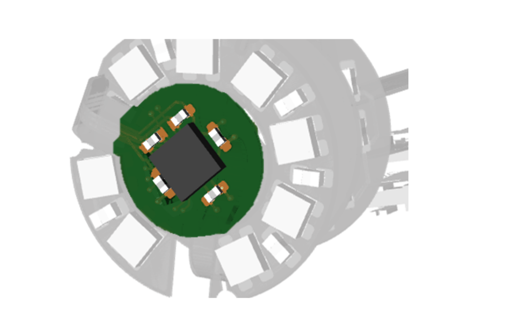
Design: BGA pitch 0,35 mm, stiffener for reinforcement, for component assembly with cavity in solder carrier
Fig.2
Design: BGA sensor fanout
Design: unbalanced coaxial connector 50R
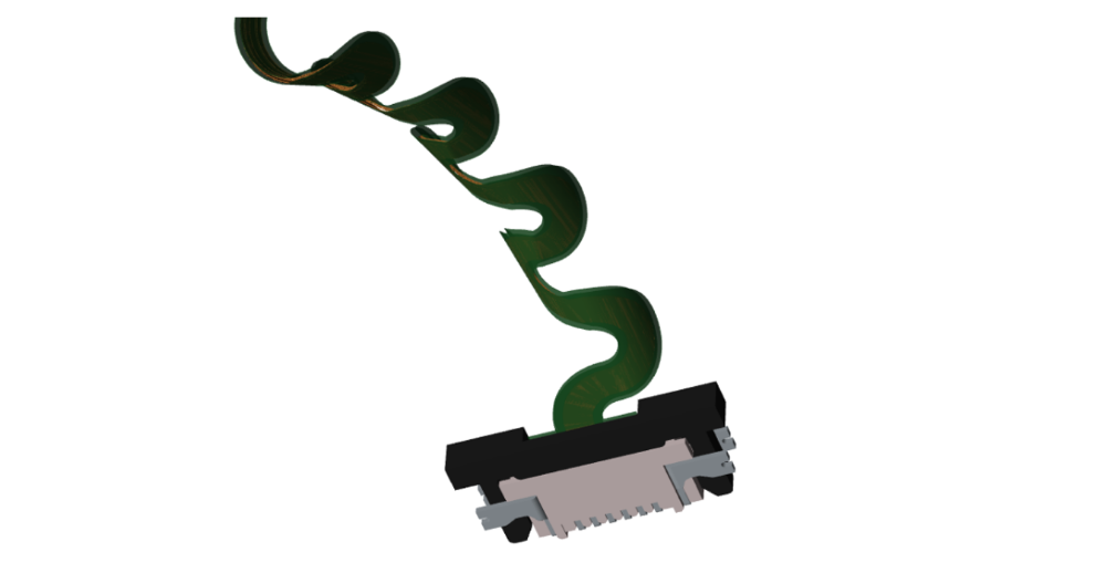
Explanation: For ZIF connector 0.2 mm +/- 0.03 mm, optionally 0.3 mm by stiffener
Design: Flexible cantilever, bendable in all spatial directions
Explanation: see www.we-online.com/slimflexsample
Detaching the SLIM.flex physical PCB sample from solder carrier
How do I design ultra-small circuits in my ECAD tool?
What options do I have for connecting the tracks to pads in the layout?
Our digital hand sample WE.scope provides an initial answer to these questions. Take a look for yourself: We have put together a sample project for you in Cadence. You can also download the documentation as Step file or in IPC-2581 format and import it into your ECAD tool.


