IC-Hersteller (104)
- Alle Hersteller
 Analog Devices
 Infineon Technologies
 Microchip
 Onsemi
 Renesas
 ROHM
ROHM STMicroelectronics
 Texas Instruments
- 3peak incorporated (28)
- Ablic (23)
- Acco Semiconductor (1)
- Advanced Power (4)
- Allegro Microsystems (97)
- Alpha & Omega Semiconductor (37)
- AnalogySemi (3)
- AnDAPT Inc (204)
- Anpec (13)
- AXElite (2)
- Backward (6)
- Bright Power Semiconductor (1)
- Broadcom (45)
- Cambridge GaN Devices (18)
- Chipanalog Micro (10)
- Cologne Chips (1)
- Convenient Power (1)
- Dialog Semiconductor (12)
- Diodes Incorporated (255)
- Divimath (8)
- Elmos AG (1)
- EPC (135)
- e-Peas Semiconductors (1)
- Eta Solutions Co. Ltd. (9)
- GaN Systems (8)
- GaNPower (3)
- Giantec (1)
- Gstek Wuxi (1)
- Helix Semiconductor (7)
- IKON (1)
- Indie Semiconductor (8)
- Innovision Semiconductor Inc (2)
- Intel (68)
- Inventchip Technology (3)
- ISSI (51)
- JoulWatt (20)
- KDPOF (3)
- Kinetic Technology (8)
- Lattice semiconductor Corporation (30)
- Littelfuse (1)
- Lumissil Microsystems (8)
- M3 Technology (M3Tek) (7)
- Macnica (22)
- Marvell Semiconductor (1)
- MaxLinear (181)
- Menlo Micro (1)
- MikroE (21)
- MindCet (2)
- Monolithic Power Systems (979)
- Navitas Semiconductor Inc (6)
- NewEdge Technologies, Inc. (1)
- Nexperia (263)
- Nisshinbo Micro Device Inc. (10)
- Nordic Semiconductor (1)
- Novosense Micro (1)
- NXP (327)
- O2 Micro International Ltd (10)
- On Bright (7)
- Panasonic (2)
- PN Junction Semiconductor (2)
- Power Integrations (120)
- Powermat (1)
- Pulsiv (19)
- Qorvo (95)
- Realsil SuRealsil(tek) Microelectronics (1)
- Richtek (297)
- Sanken Electric Co., Ltd. (16)
- Sckipio (6)
- Semtech (87)
- SG-Micro (49)
- SiFive (2)
- Silanna Semiconductor (9)
- Silergy Corporation (33)
- Silicon Laboratory Inc. (103)
- Silicontent Technology (59)
- Silvertel (61)
- Skycore Semiconductors (1)
- Skyworks (33)
- Southchip (8)
- Summit Wireless (1)
- Tagore Tech (7)
- Taiwan Semiconductor (1)
- TDK Corporation (1)
- Tempo Semiconductor (1)
- Torex (37)
- Toshiba (25)
- Transphorm (21)
- TransSIP (2)
- Union (21)
- uPI Semiconductor (2)
- Valens Semiconductor (30)
- Wise Integration (1)
- Wolfspeed (23)
- Xilinx (22)
- XL Semiconductor (3)
- XYSemi (62)
Analog Devices LTC3313 | Demoboard EVAL-LTC3313
LTC3313 5 V, 15 A Synchronous Step-Down Silent Switcher in 3 mm × 3 mm LQFN
Details
| Topologie | Abwärtswandler |
| Eingangsspannung | 2.25-5.5 V |
| Schaltfrequenz | 1800-2200 kHz |
| Ausgang 1 | 1.22 V / 15 A |
Beschreibung
The EVAL-LTC3313EV-A-Z features the LTC3313, 15 A low voltage synchronous step-down Silent Switcher® that operates as a 2 MHz,2.25 V to 5.5 V input, 1.2 V, 15 A output buck regulator. The LTC3313 supports an output voltage (VOUT) from 0.5 V to the input voltage (VIN) with operating frequencies from 500 kHz up to 5 MHz. The LTC3313 is a compact, ultralow emission, high-efficiency, and high speed synchronous monolithic step-down switching regulator. The Silent Switcher technology optimizes fast-current loops and makes it easier to minimize electromagnetic interference (EMI) and electromagnetic compatibility (EMC) emissions. The minimum on-time of 35 ns typical enables high VIN to low VOUT conversion at a high frequency.The EVAL-LTC3313EV-A-Z runs in forced continuous mode with a 2 MHz switching frequency (fSW); however, it can be configured to run at different switching frequencies or in pulse-skipping mode. The LTC3313 oscillator can also synchronize to an external clock using a MODE/SYNC turret, with the EVAL-LTC3313EV-A-Z default setup. Figure 4 shows the efficiency and power loss of the EVALLTC3313EV-A-Z with a 3.3 V input in both operation modes.The EVAL-LTC3313EV-A-Z also has an EMI filter to reduce conducted EMI. This EMI filter can be included by applying the input voltage at the VIN EMI terminal. The EMI performance of the board-EVAL-LTC3313EV-A-Z is shown in the EMI Test Results section. The red lines in the EMI performance graphs illustrate the CISPR25 Class 5 peak limits for the conducted and radiated emission tests.The LTC3313 data sheet gives a complete description of the device and its application information. The data sheet must be read in conjunction with this evaluation board user guide. The LTC3313 is assembled in a 3 mm × 3 mm LQFN package with an exposed pad for low thermal resistance. The layout recommendations for low EMI operation and maximum thermal performance are available in the LTC3313 data sheet.
Eigenschaften
- EVAL-LTC3313EV-A-Z evaluation board
- Transient circuit included for load transient evaluation
- EMI filter included to reduce noise in EMI emission tests
- MODE pin pull-up option for pulse-skipping mode evaluation
Typische Anwendungen
- Distributed DC Power Systems (POL), FPGA, ASIC, μP Core Supplies, Telecom Power supplies
- Communications, Servers
- Automotive
Weiterführende Informationen
Artikeldaten
| Artikel Nr. | Datenblatt | Simulation | Downloads | Status | Produktserie | Z @ 100 MHz (Ω) | Zmax (Ω) | Testbedingung Zmax | IR (mA) | Z @ 1 GHz (Ω) | H (mm) | Typ | Pins (pcs) | Raster (mm) | Reihen | Gender | Verpackung | Muster | |
|---|---|---|---|---|---|---|---|---|---|---|---|---|---|---|---|---|---|---|---|
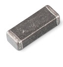 | 74279226101 | SPEC | 10 Dateien | Aktiv i| Produktion ist aktiv. Erwartete Lebenszeit: >10 Jahre. | WE-MPSB EMI Multilayer Power Suppression Bead | 100 | 160 | 1100 MHz | 8000 | 150 | 2.3 | Hochstrom | – | – | – | – | – | ||
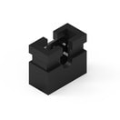 | 60800213421 | SPEC | – | 3 Dateien | Aktiv i| Produktion ist aktiv. Erwartete Lebenszeit: >10 Jahre. | WR-PHD Jumper | – | – | – | 3000 | – | – | – | 2 | 2 | – | Jumper | Beutel | |
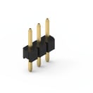 | 62000311121 | SPEC | – | 7 Dateien | Aktiv i| Produktion ist aktiv. Erwartete Lebenszeit: >10 Jahre. | WR-PHD Pin Header | – | – | – | 2000 | – | – | Gerade | 3 | 2 | Single | Stiftleiste | Beutel |
| Artikel Nr. | Datenblatt | Simulation | |
|---|---|---|---|
| 74279226101 | SPEC | |
| 60800213421 | SPEC | – |
| 62000311121 | SPEC | – |
| Muster |
|---|
| Artikel Nr. | Datenblatt | Simulation | Downloads | Status | Produktserie | Z @ 100 MHz (Ω) | Zmax (Ω) | Testbedingung Zmax | IR (mA) | Z @ 1 GHz (Ω) | H (mm) | Typ | Pins (pcs) | Raster (mm) | Reihen | Gender | Verpackung | Muster |
|---|
