Onsemi NCP4354A | Demoboard NCP4354AADAPGEVB
65 W Off-Line Adapter Featuring Very Low No-Load Power Consumption Evaluation Board User's Manual
Details
| Topologie | Sperrwandler |
| Eingangsspannung | 85-265 V |
| Ausgang 1 | 19 V / 3.5 A |
Beschreibung
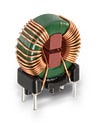
The primary side uses a flyback topology, providing theadvantage of a cost effective power stage design. The powerstage operates in both CCM (continuous conduction mode)and DCM (discontinuous conduction mode), allowing it toaccept a wide universal input voltage range. The CCMoperation provides desired full load performance with goodefficiency and low ripple of primary current. The DCMoperation then permits an increase of efficiency under thelight load conditions, by decreasing the switching losses.The device switches at 65 kHz which represents a goodtrade-off between switching losses and magnetic core size.The adapter primary side consists of several importantsections. The first is an input EMI filter to reduce theconducted EMI to the ac line at the input of the adapter. TheEMI filter is formed by common-mode inductors L3 andcapacitors C1, C2, C3 and C11 with differential modeinductor L2. The varistor R7 is used to protect the adapteragainst the line overvoltage peaks. When the power supplyis disconnected from the AC mains, X capacitors C2, C13and Y capacitors C3 and C4 are discharged through HV pinvia the following path: rectifying diodes D101, D103, surgeprotection T network R100, R101 and C100. This featurereplaces commonly used discharging resistors and savesapproximately 25 mW of input power consumption at230 Vac. The next block is the rectifier with bulk capacitor.The main power stage of the flyback converter utilizes thelow RDSon MOSFET SPP11N60C3 along with a customdesigned transformer TR1 KA5038-BL from Coilcraft. Thedetailed design procedure of a flyback adapter can be foundin the application note AND8461/D at ON SemiconductorSecondary rectification is done by a low forward voltagedrop Schottky diode NTST30100SG fromON Semiconductor. A simple RC snubber across thesecondary rectifier damps the high frequency ringing causedby the unclamped leakage inductance of the secondary sideof the transformer and the rectification diode capacitance.Secondary controller NCP4354A provides the outputvoltage and output current regulation. Output voltage is setby voltage divider R112, R117, R118 and R127, outputcurrent is sensed at sense resistor R111. Regulation outputis coupled to the NCP1246 primary side controller via theoptocoupler. The NCP4354 secondary controller alsodetects very light load condition via D105, R114, C106,R115 and R116 by OFFDET pin. When light load conditionis detected, the primary controller is switched into OFFmode by ON/OFF current sink to DRIVE pin viaoptocoupler. The built in LED driver indicates primary sideoperation (when SMPS is not in OFF mode). The LEDdriver switches with 1 kHz frequency and 12% duty cycle inorder to optimize LED efficiency.
Eigenschaften
Constant Voltage Constant Current Regulation (CCCV)
- Very Low Input Power at Light and No Load
- High Efficiency Across the Entire Load Range
- Overpower Protection
- Universal Mains Operation
Weiterführende Informationen
Artikeldaten
| Artikel Nr. | Datenblatt | Simulation | Downloads | Status | Produktserie | Ø Kabel max. (mm) | Ø OD (mm) | Ø ID (mm) | Z @ 25 MHz 1 Windung (Ω) | Z @ 100 MHz 1 Windung (Ω) | IR (A) | L (µH) | RDC max. (mΩ) | VR (V (AC)) | VT (V (AC)) | Material | L (mm) | W (mm) | H (mm) | Montageart | Muster | |
|---|---|---|---|---|---|---|---|---|---|---|---|---|---|---|---|---|---|---|---|---|---|---|
 | 74270073 | SPEC | 2 Dateien | Aktiv i| Produktion ist aktiv. Erwartete Lebenszeit: >10 Jahre. | WE-SAFB | 1 | 3.5 | 1.2 | 30 | 53 | – | – | – | – | – | 7 W 850 | 4 | – | 3.8 | – | ||
 | 744841414 | SPEC | 9 Dateien | Aktiv i| Produktion ist aktiv. Erwartete Lebenszeit: >10 Jahre. | WE-CMB NiZn Stromkompensierte Netzdrossel | – | – | – | – | – | 4 | 14 | 15 | 250 | 1500 | NiZn | 16 | 7.5 | 17.5 | THT | ||
 | 7447018 | SPEC | – | 8 Dateien | Aktiv i| Produktion ist aktiv. Erwartete Lebenszeit: >10 Jahre. | WE-FI Funkentstördrossel | – | – | – | – | – | 2.5 | 150 | 100 | – | – | – | 16.5 | 10.7 | – | THT |
| Muster |
|---|
| Artikel Nr. | Datenblatt | Simulation | Downloads | Status | Produktserie | Ø Kabel max. (mm) | Ø OD (mm) | Ø ID (mm) | Z @ 25 MHz 1 Windung (Ω) | Z @ 100 MHz 1 Windung (Ω) | IR (A) | L (µH) | RDC max. (mΩ) | VR (V (AC)) | VT (V (AC)) | Material | L (mm) | W (mm) | H (mm) | Montageart | Muster |
|---|


