Characteristics
- Hybrid material with absorber and metal layers, effective both against magnetic and electric fields
- Wide frequency range from 100 Hz up to 25 GHz
- Extremely flexible
- Very low thickness: 0.072 mm
- Isolated version with high surface resistance
- Non-isolated version which allows the connection of the metal layer to ground, housing,…
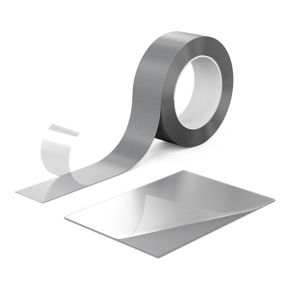
- With self-adhesive backing for easy installation
- Absorber layer with permeability of 100
- Metal layer: Aluminum
- Operating temperature: -25 up to +105°C
- Easy to process
- Custom designs on request
- Permeability
- Shape and size
- Metal layer
- Thickness
- Isolation
- Adhesive
- Permeability
Applications
- Alternative to classical Shielding Cabinet solution, providing similar levels of shielding effectiveness
- EMC noise suppresion
- Magnetic Decoupling
- SAR reduction
- Avoiding cavity resonances
- Prevention of Electro Static Discharge
- Housing and openings between PCB's, on IC's, processors and controllers, on cables which need high flexibility and LCD/LED monitors.
- Useful for any kind of electronic device
Products
| Order Code | Datasheet | Simulation | Downloads | Status | µʹ @ 1 MHz | L (mm) | W (mm) | H (mm) | Version | Samples |
|---|---|---|---|---|---|---|---|---|---|---|
| 371000 | SPEC | 3 files | New i| Product is new in our portfolio and production is active. Expected lifetime: >10 years. | 100 | 15000 | 50 | 0.072 | Non-Isolated | ||
| 371001 | SPEC | 3 files | New i| Product is new in our portfolio and production is active. Expected lifetime: >10 years. | 100 | 105 | 74 | 0.072 | Non-Isolated | ||
| 371002 | SPEC | 3 files | New i| Product is new in our portfolio and production is active. Expected lifetime: >10 years. | 100 | 297 | 210 | 0.072 | Non-Isolated | ||
| 371100 | SPEC | 3 files | New i| Product is new in our portfolio and production is active. Expected lifetime: >10 years. | 100 | 15000 | 50 | 0.072 | Isolated | ||
| 371101 | SPEC | 3 files | New i| Product is new in our portfolio and production is active. Expected lifetime: >10 years. | 100 | 105 | 74 | 0.072 | Isolated | ||
| 371102 | SPEC | 3 files | New i| Product is new in our portfolio and production is active. Expected lifetime: >10 years. | 100 | 297 | 210 | 0.072 | Isolated |
| Samples |
|---|
| Order Code | Datasheet | Simulation | Downloads | Status | µʹ @ 1 MHz | L (mm) | W (mm) | H (mm) | Version | Samples |
|---|
One for all solution
One for all solution
The EMI Patch is a universal solution with wider frequency range and higher attenuation than conventional absorber sheets and additional heat dissipation.
The combination of absorber and metal layer enables a new level of board level shielding. Stray fields are absorbed whereby nearly same perfomance as with the help of shielding cabinets is achieved.
Available in sheet form or on a roll, it is the perfectly adaptable solution for testing, EMC labs and also final production. With less than 0.1 mm thickness the EMI patch is suitable for applications with limited height.

How it works

If the magnetic layer is used alone, it attenuates EMI.

With the metal layer, electromagnetic interference is attenuated, but it triggers eddy currents that lead to magnetic leakage.

By combining the metal with the magnetic layer, not only it does not re-radiate, but also this combination decreases largely the level of electromagnetic radiated emissions measured in the near field.

The metal layer in the EMI Patch functions as a ground reference plane when connected to GND.
- When installing, make sure that the metal layer is on the top.
- Mounting the EMI Patch onto the component is made simple with its adhesive tape layer.
- Employing shielding tape (WE-CF) ensures a low-impedance ground connection.


Thanks to the metal layer the EMI Patch has a good thermal coductivity and thus helps to dissipate heat. The aluminum layer is able to spread the heat through its whole surface, being more effective in thermal management than a common absorber sheet.

