Analog Devices LTM4681 | Demoboard DC2924A-B
Quad 31.25A or Single 125A μModule Regulator with Digital Power System Management
Overview
| Topology | Buck Converter |
| Input voltage | 4.5-16 V |
| Output 1 | 1 V / 30 A |
Description
Demonstration circuit 2924A-A/2924A-B features the LTM4681: the wide input and output voltage range, high efficiency and power density, quad output PolyPhase® DC/DC step-down μModule® regulator with digital power system management. Demo board DC2924A is available in two versions: DC2924A-A is configured as 4-phase 4 outputs, DC2924A-B is configured as 4-phase single output. The demo board default input voltage range is 4.5V to 16V. However, if VIN is lower than 6V and within 4.5V ≤ VIN ≤ 5.75V range, minor modification to certain existing onboard components is required. Please refer to the Operation at Low VIN: 4.5V ≤ VIN ≤ 5.75V paragraph in the demo manual for more details. The factory default output voltage (VOUT0, VOUT1, VOUT2 and VOUT3) is 1V at 30A maximum load current per channel (DC2924A-A). The factory default output voltage VOUT = 1V at 120A maximum load current (DC2924A-B). Each channel can deliver up to 30A maximum load current but forced airflow and heat sink might also be used to further optimize the output power when all output rails are on and fully loaded. The demo board output voltages can be adjusted from 0.6V up to 1.8V. Programming the output voltages to any value that is greater than 1.8V, requires derating output current based on thermal derating curves provided in the LTM4681 data sheet. The factory default switching frequency is preset at 350kHz typical. Both versions of DC2924A come with PMBus interface and digital power system management functions. An onboard 12-pin connector is available for users to connect the dongle DC1613A to the demo board, provides an easy way to communicate and program the part using LTpowerPlay® software development tool. LTpowerPlay software and I2C/PMBus/SMBus dongle DC1613A allows users to monitor real time telemetry of input and output voltages, input and output current, switching frequency, internal IC die temperatures, external power component temperatures and fault logs. Programmable parameters include device address, output voltages, control loop compensation, switching frequency, phase interleaving, DCM or CCM mode of operation, digital soft-start, sequencing and time based shutdown, fault responses to input and output overvoltage, output overcurrent, IC die and power component overtemperatures.
Features
- Quad Digitally Adjustable Analog Loops with Digital Interface for Control and Monitoring
- Wide Input Voltage Range: 4.5V to 16V
- Output Voltage Range: 0.5V to 3.3V
- ±0.5% Maximum DC Output Error Over Temperature
- ±4% Current Readback Accuracy: 0°C to 125°C
- Integrated Input Current Sense Amplifier
- 400kHz PMBus-Compliant I2C Serial Interface
- Supports Telemetry Polling Rates Up to 125Hz
- Integrated 16-Bit ΔΣ ADC
- Parallel and Current Share Multiple Modules
- 15mm × 22mm × 8.17mm BGA Package
- Readable Data:
- Input and Output Voltages, Currents, and Temperatures
- Running Peak Values, Uptime, Faults and Warnings
- Onboard EEPROM Fault Log Record
- Writable Data and Configurable Parameters:
- Output Voltage, Voltage Sequencing and Margining
- Digital Soft-Start/Stop Ramp, Program Analog Loop
- OV/UV/OT, UVLO, Frequency and Phasing
Typical applications
- Communication, data center
- Industrial automation technology, Instrument and measurement
More information
Products
| Order Code | Datasheet | Simulation | |
|---|---|---|---|
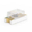 | 150060GS75000 | SPEC | |
 | 150060RS75000 | SPEC | |
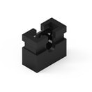 | 60800213421 | SPEC | – |
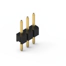 | 62000311121 | SPEC | – |
| Samples |
|---|
| Order Code | Datasheet | Simulation | Downloads | Status | Product series | λDom typ. (nm) | Emitting Color | λPeak typ. (nm) | IV typ. (mcd) | VF typ. (V) | Chip Technology | 2θ50% typ. (°) | Pins (pcs) | Pitch (mm) | Rows | H (mm) | Gender | Type | IR (A) | Packaging | Samples |
|---|


