IC manufacturers NXP

IC manufacturers (98)

NXP LPC55S6x | Demoboard FRDM-MCXN947

High Efficiency Arm® Cortex®-M33-Based Microcontroller Family

Overview

TopologyFPGA
IC revisionA

Description

The LPC55S6x MCU family is part of the EdgeVerse™ edge computing platform and builds on the world’s first general-purpose Cortex-M33 based microcontroller introduced with the LPC5500 series. This high-efficiency family, inclusive of LPC55S69JBD100, LPC55S66JBD100, LPC55S69JEV98, LPCS66JEV98, LPC55S69JBD64, LPCS66JBD64 MCUs, leverages the new Armv8-M architecture to introduce new levels of performance and advanced security capabilities including TrustZone-M and co-processor extensions. The LPC55S6x family enables these co-processors extensions and leverages them to bring significant signal processing efficiency gains from a proprietary DSP accelerator offering a 10x clock cycle reduction. An optional second Cortex-M33 core offers flexibility to balance high performance and power efficiency.In addition, the LPC55S6x MCU family provides benefits from 40nm NVM based process technology cost advantages, broad scalable packages, and memory options, as well as a robust enablement including MCUXpresso Software and Tools ecosystem and low-cost development boards.

Features

Arm Cortex-M33 CoreArm Cortex-M33 processor, running at a frequency of up to 150 MHzTrustZone, floating point unit (FPU) and memory protection unit (MPU)Arm Cortex-M33 built-in nested vectored interrupt controller (NVIC)Non-maskable interrupt (NMI) input with a selection of sourcesCo-ProcessorArm Cortex-M33 co-processorRunning at a frequency of up to 150 MHzThe configuration of this instance does not include MPU, FPU, DSP, ETM, and TrustZoneSystem tick timerCASPER crypto co-processor to enable hardware acceleration for certain asymmetric cryptographic algorithmsPowerQuad hardware accelerator for (fixed and floating point) DSP functionsOn-Chip MemoryUp to 640 KB on-chip flash program memory with a flash accelerator and 512-byte page erase and writeUp to 320 KB total SRAM consisting of 288 KB on the system bus and 32 KB on code busSecurity FeaturesArm TrustZone enabledPRINCE module for real-time encryption of data being written to on-chip flash and decryption of encrypted flash data during reading to allow asset protectionAES-256 encryption/decryption engineSecure hash algorithm (SHA2) module supporting secure boot with dedicated DMA controllerPhysical unclonable function(PUF) using dedicated SRAM for silicon fingerprint. PUF can generate, store, and reconstruct key sizes from 64 to 4096 bits. Includes hardware for key extractionRandom number generator (RNG)128-bit unique device serial number for identification (UUID)Secure GPIOThe LPC55S6x is part of the EdgeLock ™ Assurance program.Serial InterfacesFlexcomm Interface contains up to nine serial peripherals. Each Flexcomm Interface can be selected by software to be a USART, SPI, I2C, and I2S interfaceI2C-bus interfaces support fast-mode and fast-mode plus with data rates of up to 1 Mbit/s and with multiple address recognition and monitor modeUSB 2.0 full speed host/device controller with on-chip PHY and dedicated DMA controller supporting crystal-less operation in device modeUSB 2.0 high-speed host/device controller with on-chip high-speed PHYDigital PeripheralsDMA0 controller with 23 channels and up to 22 programmable triggers, able to access all memories and DMA-capable peripheralsDMA1 controller with 10 channels and up to 16 programmable triggers, able to access all memories and DMA-capable peripheralsSecured digital input/output (SD/MMC and SDIO) card interface with DMA support. SDIO with support for up to two cards. Supported card types are MMC, SDIO, and CE-ATA. Supports SD2.0, and SR25CRC engine block can calculate a CRC on supplied data using one of three standard polynomials with DMA supportUp to 64 general-purpose input/output (GPIO) pinsGPIO registers are located on the AHB for fast access. The DMA supports GPIO portsUp to eight GPIOs can be selected as Pin Interrupts (PINT), triggered by rising, falling or both input edgesTwo GPIO Grouped Interrupts (GINT) enable an interrupt based on a logical (AND/OR) combination of input statesI/O pin configuration with support for up to 16 function options.Programmable logic unit (PLU) to create small combinational and/or sequential logic networks including state machinesAnalog Peripherals16-bit ADC with five differential channel pair (or 10 singled-ended channels), and with multiple internal and external trigger inputs and sample rates of up to 1.0 M Samples/sec. The ADC supports two independent conversion sequencesIntegrated temperature sensor connected to the ADCComparator with five input pins and external or internal reference voltageTimersFive 32-bit standard general purpose asynchronous timers/counters, which support up to four capture inputs and four compare outputs. Specific timer events can be selected to generate DMA requestsOne SCTimer/PWM with eight input and ten output functions (including capture and match). Inputs and outputs can be routed to or from external pins and internally to or from selected peripherals. Internally, the SCTimer/PWM supports 16 match/captures, 16 events, and 32 states32-bit Real-time clock (RTC) with 1 s resolution running in the always-on power domain. A timer in the RTC can be used for wake-up from all low power modes including deep power-down, with 1 ms resolutionMultiple-channel multi-rate 24-bit timer (MRT) for repetitive interrupt generation at up to four programmable, fixed ratesWindowed watchdog timer (WWDT) with FRO 1 MHZ as a clock sourceMicro-tick timer running from the watchdog oscillator can be sued to wake-up the device from sleep and deep-sleep modes42-bit free running OS timer as continuous time-base for the system, available in any reduced power modes.Clock GenerationInternal free running oscillator (FRO). This oscillator provides a selectable 96 MHz output, and a 12 MHz output (divided down from the selected higher frequency) that can be used as a system clock. The FRO is trimmed to +/- 1% accuracy over the entire voltage and temperature range32 kHz internal free running oscillator FRO. The FRO is trimmed to +/- 1% accuracy over the entire voltage and temperature rangeInternal low power oscillator (FRO 1 MHz)Crystal oscillator with an operating frequency of 1 MHz to 25 MHz. Option for external clock input (bypass mode) for clock frequencies of up to 25 MHzCrystal oscillator with 32.768 kHz operating frequencyPLL0 and PLL1 allows CPU operation up to the maximum CPU rate without the need for a high-frequency external clockClock output function with divider to monitor internal clocksFrequency measurement unit for measuring the frequency of any on-chip or off-chip clock signalPower-Saving ModesIntegrated power management unit (PMU) to minimize power consumptionReduced power modes: Sleep, deep-sleep with RAM retention, power-down with RAM retention and CPU0 retention, and deep power-downConfigurable wake-up options from peripheral interruptsThe micro-tick timer running from the watchdog oscillator, and the real-time clock (RTC) running from the 32.678 kHz clock, can be used to wake-up the device from sleep and deep-sleep modesPower-on reset (POR)Brown-out-detect (BOD) with separate thresholds for interrupt and forced resetAdditional InformationOperating from an internal DC-DC converterSingle power supply 1.8 V to 3.6 VJTAG boundary scan supportedOperating temperature range -40 °C to +105 °CAvailable in HLQFP100, VFBGA98, and HTQFP64 packages

Typical applications

  • Permanent Magnet Synchronous Motor (PMSM)
  • Vital Signs Monitors
  • Industrial HMI
  • Smart Appliance
  • Air Conditioning (AC)
  • AI and Machine Learning
  • Electricity Meter
  • Smart Lock
  • Brushless DC Motor (BLDC) Control
  • Home Security and Surveillance
  • Motor Drives
  • Factory Automation
  • Home Control and Security
  • Building Control

Products

Order Code Data­sheet Simu­lation Downloads Status Product seriesλDom typ.
(nm)
Emitting ColorλPeak typ.
(nm)
IV typ.
(mcd)
VF typ.
(V)
Chip Technology50% typ.
(°)
ApplicationfTol. fStability
(ppm)
Cload
(pF)
Operating TemperatureCTol. CVR
(V (DC))
SizeDF
(%)
RISOCeramic TypeL
(mm)
W
(mm)
H
(mm)
Fl
(mm)
PackagingZ @ 100 MHz
(Ω)
Zmax
(Ω)
Test Condition ZmaxIR 2
(mA)
RDC max.
(Ω)
Type Samples
150040SS73240SPEC
7 files Active i| Production is active. Expected lifetime: >10 years.WL-SMCC SMT Mono-color Chip LED Compact 630 Super Red 645 75 2 AlInGaP 120 -40 °C up to +85 °C 0402
742792651SPEC
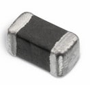
9 files Active i| Production is active. Expected lifetime: >10 years.WE-CBF SMT EMI Suppression Ferrite Bead -55 °C up to +125 °C 0603 1.6 0.8 0.8 0.3 600 800 200 MHz 1000 0.2 High Current
885012205037SPEC
6 files Active i| Production is active. Expected lifetime: >10 years.WCAP-CSGP MLCCs 16 V(DC) -55 °C up to +125 °C100 nF ±10% 16 0402 55 GΩ X7R Class II 1 0.5 0.5 0.25 7" Tape & Reel
885012106017SPEC
8 files Active i| Production is active. Expected lifetime: >10 years.WCAP-CSGP MLCCs 16 V(DC) -55 °C up to +85 °C1 µF ±20% 16 0603 100.1 GΩ X5R Class II 1.6 0.8 0.8 0.4 7" Tape & Reel
830064296SPEC
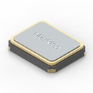
5 files Active i| Production is active. Expected lifetime: >10 years.WE-XTAL Quartz Crystal Processor, CAN, Bluetooth16 MHz ±20ppm 20 8 -10 °C up to +70 °C CFPX-180 3.2 2.5 0.8
Samples
Order Code Data­sheet Simu­lation Downloads Status Product seriesλDom typ.
(nm)
Emitting ColorλPeak typ.
(nm)
IV typ.
(mcd)
VF typ.
(V)
Chip Technology50% typ.
(°)
ApplicationfTol. fStability
(ppm)
Cload
(pF)
Operating TemperatureCTol. CVR
(V (DC))
SizeDF
(%)
RISOCeramic TypeL
(mm)
W
(mm)
H
(mm)
Fl
(mm)
PackagingZ @ 100 MHz
(Ω)
Zmax
(Ω)
Test Condition ZmaxIR 2
(mA)
RDC max.
(Ω)
Type Samples