Onsemi NCP10672 | Demoboard 4 Watt Non-isolated Power Supply DN05129/D
Universal AC Input, 4 Watt Non-isolated Power Supply
Overview
| Topology | Buck Converter |
| Input voltage | 90-265 V |
| Output 1 | 15 V / 0.27 A |
| IC revision | 1.0 |
Description
This design note describes a simple 4 W, universal AC input, non-isolated buck converter. The key parameters of the power supply are dimensions and fast transient respond with given output filter. It is recommended to modify the power supply to fit individual needs, like standby consumption, output voltage ripple etc. The power supply is a simple non-isolated buck topology utilizing ON Semiconductor’s new NCP10672 monolithic switcher with integrated 12 ohm MOSFET in a SOIC7 package (IC1). This Design Note provides the complete circuit schematic and BOM. The AC voltage is rectified (D4, D5, D6, D8) and connected to bulk capacitor C4. The rising voltage allows DSS to charge Vcc capacitor C8. Once the voltage on C8 crosses UVLO level, the NCP10672 starts switching. When the internal MOSFET is on, the current flows from C4 to Drain pin, from GND pin through L2 into C3, then via negative line back to C4. When the MOSFET is turned off, the current flows from L2 to C3, then via D3 back to the coil. During demagnetization period, C1 is charged to output voltage level (through D2). The C1 value affects no load consumption, transient response etc. The reason is, the capacitor can only be charged via D2, but discharging is done by FB resistor divider. Moreover, the charging is done only during demagnetization period of L2. If lower value of C1 is used, in skip mode, the C1 is discharged faster, so IC1 switches frequently to check the output value. On the other hand, choosing a bigger C1 value results in a longer switching period. As a result, the higher value of C1 decreases no load consumption and improves load regulation (see Figure 6 and Figure 7). The lower value of C1 decreases transient response time (see Figure 13 and Figure 14). The C1 value selection depends on designer’s priorities. A resistor divider composed of R5, R6 and R3 reduces voltage for FB pin (3.3 V). The OVP protection and supplying the IC is done by R4 and D7 from the output voltage. Compensation network composes of R2, C2 and C7. The output diode D1 is a dummy load to clamp high output voltage in no load or low load conditions. The output power can be boosted up to 7.5 W @ 230 V if C4 and C3 capacitances are increased. If such power is drawn from the demo without any update, the output ripple will rise.
Features
- Universal AC input range (90 – 265 Vac).
- Small dimensions.
- Low no load consumption (it requires a device change)
- Over-voltage and over temperature protection.
- Frequency Jittering for Better EMI Signature (EMI not tested).
Typical applications
- Non-isolated Power Supply
More information
Products
| Order Code | Datasheet | Simulation | Downloads | Status | Product series | L (µH) | IRP,40K (A) | ISAT (A) | RDC max. (mΩ) | fres (MHz) | Size | Version | IR (A) | Samples | |
|---|---|---|---|---|---|---|---|---|---|---|---|---|---|---|---|
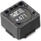
 | 7687709681 | SPEC | 10 files | Active i| Production is active. Expected lifetime: >10 years. | WE-PD HV SMT Power Inductor (High Voltage) | 680 | – | 1.2 | 1150 | 1.5 | 1210 | – | 0.8 | ||
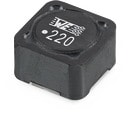
 | 744777930 | SPEC | 9 files | Active i| Production is active. Expected lifetime: >10 years. | WE-PD SMT Power Inductor | 1000 | 0.37 | – | 6000 | 2.2 | 7345 | Robust | 0.2 |
| Order Code | Datasheet | Simulation | |
|---|---|---|---|
 | 7687709681 | SPEC | |
 | 744777930 | SPEC |
| Samples |
|---|
| Order Code | Datasheet | Simulation | Downloads | Status | Product series | L (µH) | IRP,40K (A) | ISAT (A) | RDC max. (mΩ) | fres (MHz) | Size | Version | IR (A) | Samples |
|---|


