Lattice semiconductor Corporation LFE5UM-45F-8BG381IES | Demoboard LFE5UM-45F-8BG381IES
ECP5™ Family Data Sheet
Overview
| Topology | Other Topology |
| IC revision | 1.3 |
Description
The ECP5 family of FPGA devices is optimized to deliver high performance features such as an enhanced DSP architecture, high speed SERDES and high speed source synchronous interfaces in an economical FPGA fabric. This combination is achieved through advances in device architecture and the use of 40nm technology making thedevices suitable for high-volume, high-speed, low-cost applications.The ECP5 device family covers look-up-table (LUT) capacity to 84K logic elements and supports up to 365 user I/Os.The ECP5 device family also offers up to 156 18 x 18 multipliers and a wide range of parallel I/O standards.The ECP5 FPGA fabric is optimized high performance with low power and low cost in mind. The ECP5 devices utilize reconfigurable SRAM logic technology and provide popular building blocks such as LUT-based logic, distributedand embedded memory, Phase Locked Loops (PLLs), Delay Locked Loops (DLLs), pre-engineered source synchronous I/O support, enhanced sysDSP slices and advanced configuration support, including encryption anddual-boot capabilities.The pre-engineered source synchronous logic implemented in the ECP5 device family supports a broad range of interface standards, including DDR2/3, LPDDR2/3, XGMII and 7:1 LVDS.The ECP5 device family also features high speed SERDES with dedicated PCS functions. High jitter tolerance and low transmit jitter allow the SERDES plus PCS blocks to be configured to support an array of popular data protocols including PCI Express, Ethernet (XAUI, GbE, and SGMII) and CPRI. Transmit De-emphasis with pre- andpost- cursors, and Receive Equalization settings make the SERDES suitable for transmission and reception over various forms of media.The ECP5 devices also provide flexible, reliable and secure configuration options, such as dual-boot capability, bitstream encryption, and TransFR field upgrade features.The Lattice Diamond™ design software allows large complex designs to be efficiently implemented using the ECP5 FPGA family. Synthesis library support for ECP5 devices is available for popular logic synthesis tools. TheDiamond tools use the synthesis tool output along with the constraints from its floor planning tools to place and route the design in the ECP5 device. The tools extract the timing from the routing and back-annotate it into the design for timing verification.Lattice provides many pre-engineered IP (Intellectual Property) modules for the ECP5 family. By using these configurable soft core IPs as standardized blocks, designers are free to concentrate on the unique aspects of theirdesign, increasing their productivity.
Features
- Higher Logic Density for Increased SystemIntegration
- 24K to 84K LUTs
- 197 to 365 user programmable I/Os Embedded SERDES
- 270 Mbps to 3.2 Gbps for Generic 8b10b, 10-bitSERDES, and 8-bit SERDES modes
- Data Rates 270 Mbps to 3.2 Gbps per channelfor all other protocols
- Up to four channels per device: PCI Express,Ethernet (1GbE, SGMII, XAUI), and CPRI. sysDSP™
- Fully cascadable slice architecture
- 12 to 160 slices for high performance multiplyand accumulate
- Powerful 54-bit ALU operations
- Time Division Multiplexing MAC Sharing
- Rounding and truncation
- Each slice supports
— Half 36 x 36, two 18 x 18 or four 9 x 9 multipliers
— Advanced 18 x 36 MAC and 18 x 18 Multiply-Multiply-Accumulate (MMAC) operations Flexible Memory Resources
Up to 3.744 Mbits sysMEM™ Embedded BlockRAM (EBR)
194K to 669K bits distributed RAM sysCLOCK Analog PLLs and DLLs
Four DLLs and four PLLs in LFE5-45 and LFE5-85; two DLLs and two PLLs in LFE5-25 Pre-Engineered Source Synchronous I/O
DDR registers in I/O cells
Dedicated read/write levelling functionality
Dedicated gearing logic
Source synchronous standards support
— ADC/DAC, 7:1 LVDS, XGMII
— High Speed ADC/DAC devices
- Dedicated DDR2/DDR3 and LPDDR2/LPDDR3memory support with DQS logic, up to 800 Mbpsdata-rate Programmable sysI/O™ Buffer SupportsWide Range of Interfaces
- On-chip termination
- LVTTL and LVCMOS 33/25/18/15/12
- SSTL 18/15 I, II
- HSUL12
- LVDS, Bus-LVDS, LVPECL, RSDS, MLVDS
- subLVDS and SLVS, MIPI D-PHY input interfaces Flexible Device Configuration
- Shared bank for configuration I/Os
- SPI boot flash interface
- Dual-boot images supported
- Slave SPI
- TransFR™ I/O for simple field updates Single Event Upset (SEU) MitigationSupport
- Soft Error Detect – Embedded hard macro
- Soft Error Correction – Without stopping useroperation
- Soft Error Injection – Emulate SEU event todebug system error handling System Level Support
- IEEE 1149.1 and IEEE 1532 compliant
- Reveal Logic Analyzer
- On-chip oscillator for initialization and generaluse
- 1.1 V core power supply
More information
Products
| Order Code | Datasheet | Simulation | |
|---|---|---|---|
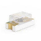 | 150060BS75000 | SPEC | |
 | 150060VS75000 | SPEC | |
 | 150060YS75000 | SPEC | |
 | 150060RS75000 | SPEC | |
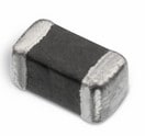 | 74279265 | SPEC | |
 | 742792602 | SPEC | |
 | 742792410 | SPEC | |
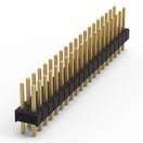 | 61304021121 | SPEC PCN pendingDue to a pending PCN, a modification of the component will be implemented soon. Please find the PCN below. If you have further questions please get in contact with our sales staff. | – |
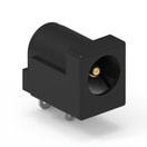 | 694106301002 | SPEC PCN pendingDue to a pending PCN there will be a new datasheet revision issued for this order code soon. Please find the actual as well based on valid PCN date the new revision datasheet below. If you have further questions please get in contact with our sales staff. | – |
 | 416131160808 | SPEC | – |
 | 430483031816 | SPEC | – |
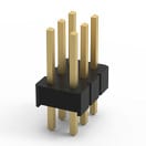 | 61300621121 | SPEC | – |
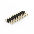 | 61301011121 | SPEC | – |
| Samples |
|---|
| Order Code | Datasheet | Simulation | Downloads | Status | Product series | λDom typ. (nm) | Emitting Color | λPeak typ. (nm) | IV typ. (mcd) | VF typ. (V) | Chip Technology | 2θ50% typ. (°) | Pins (pcs) | Center pin Ø (Value) (mm) | Plug OD (mm) | IR (mA) | Working Voltage (V (AC)) | Packaging | Pitch (mm) | Rows | Gender | Poles | L (mm) | Vaporphase process | H (mm) | Operation Force (g) | Electrical Life (Cycles) | Actuator Color | Washable | Z @ 100 MHz (Ω) | Zmax (Ω) | Test Condition Zmax | IR 2 (mA) | RDC max. (Ω) | Type | Samples |
|---|


